
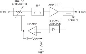
Fig. 1 Block diagram of a typical AGC solution implemented with discrete components.
Automatic gain control (AGC) or automatic power control (APC) circuits are used primarily to maintain a constant power level in the signal chain of a communication transceiver. A simple AGC circuit involves attenuation, amplification, power detection and gain control mechanisms. In an AGC system, the average output signal level is fed back to adjust the gain to an appropriate level for a range of input signal levels. For example, without AGC, the audio level emitted from an AM radio receiver would vary depending on the received signal strength; the AGC effectively reduces the volume when the signal is strong and raises it when it is weaker. AGC algorithms often use controllers that can adjust the gain of the signal chain in inverse proportion to the error between desired and measured power levels. Figure 1 shows a discrete implementation of an AGC circuit controlling gain in accordance with the power level detected via a feedback loop.
Unfortunately, AGC loops implemented with discrete components often suffer from a number of deficiencies. For example, the analog voltage variable attenuator (VVA) element in a discrete AGC loop often exhibits large OIP3 dips at certain control voltages, or OIP3 degradation as the attenuation is increased. Since the AGC loop is implemented with multiple discrete components, the power control accuracy is more sensitive to part-to-part and temperature variations. Additionally, each of these components often requires external circuitry that requires extra PCB space and further complicates the overall AGC loop design.
Hittite Microwave has developed a unique new product line of highly integrated analog AGC solutions that address many of the complex challenges of designing high performance AGC loops. Table 1 summarizes the key specifications of these new products. The HMC992LP5E is an IF analog controlled variable gain amplifier (VGA) that operates from 50 to 800 MHz, and the HMC993LP5E is an RF analog controlled gain amplifier that operates from 700 MHz to 3 GHz.
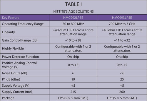

Fig. 2 HMC992LP5E gain vs. VCTRL at 100 MHz.
Both the HMC992LP5E and the HMC993LP5E combine a high performance analog VGA core with a high speed power detector in a compact 5×5 mm plastic package for a complete AGC solution. The VGA core includes two identical voltage variable attenuators followed up by two gain block amplifiers and a high accuracy log detector. The HMC992LP5E and the HMC993LP5E offer a flexible architecture, where the VGA core is configurable with 1 or 2 attenuators depending upon the dynamic range requirements. These devices can also be used either as standalone high performance VGAs in open loop configuration, or as a compact AGC solution in closed loop operation. The HMC992LP5E and HMC993LP5E AGC solutions are available in compact 25 mm² SMT packages and provide an excellent alternative to discrete AGC loops by reducing the complexity of the loop design, and the total number of components required.
The unique VGA core of the HMC992LP5E and the HMC993LP5E exhibits a well-balanced gain slope vs. control voltage characteristic over a wide range of control voltages (see Figure 2), which greatly simplifies the implementation of AGC loop configurations.
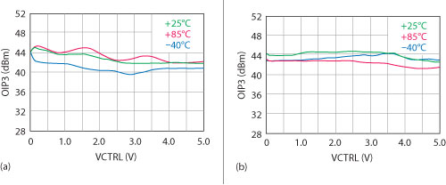
Figure 3 HMC992LP5E OIP3 vs. VCTRL at 300 MHz (a) and HMC993LP5E OIP3 vs. VCTRL at 900 MHz (b).
Another key advantage of the HMC992LP5E and the HMC993LP5E is their ability to provide constant high OIP3 over the entire attenuation range. HMC992LP5E and HMC993LP5E differentiate themselves from traditional VGAs by providing constant OIP3 at any control voltage or attenuation level. Figures 3A and 3B show that a constant OIP3 of greater than +40 dBm is achieved over the entire gain range.
The integrated power detector of the HMC992LP5E and HMC993LP5E exhibits excellent temperature stability. Both devices provide very accurate AGC closed loop power control, which is independent of part-to-part and temperature variations.
In open loop operation, VGA operation is achieved with two attenuators and two amplifiers by applying different gain voltages to the VCTRL pin. This pin is common to both attenuators in the VGA core, and operates between 1 and 4 V. Increasing the VCTRL pin voltage reduces the gain of the HMC992LP5E and HMC993LP5E VGAs and increases the input power level required for power saturation. These AGCs are well suited for transceiver applications that require a single gain or power calibration setting during the manufacturing process.
In closed loop operation, the control voltage of the attenuator is driven by the RF detector, and the output power is automatically adjusted for a given VSET value. In other words, the output power is controlled by the VSET pin (see Figure 4). In such configurations, Hittite AGCs automatically compensate for the variations over emperature and part-to-part through the high accuracy power detector, to achieve repeatable linear power adjustments. Both the HMC992LP5E and the HMC993LP5E are designed to be used in closed loop operation, require only DC blocking capacitors and resistors, and are specified for operation from -40° to +85°C.

Figure 4 HMC992LP5E output power vs. VSET over input power at 300 MHz (closed loop configuration).
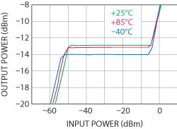
Figure 5 HMC992LP5E output power vs. input power at 400 MHz and VSET = 0.6V.
Figure 5 shows the output power vs. input power transfer characteristics of the HMC992LP5E over different temperatures for a closed AGC loop configuration when VSET is 0.6 V. The figure shows that the device exhibits over 45 dB of dynamic range with a minimal output power variation of less than 1 dB over temperature.
Hittite Microwave’s design philosophy involves choosing the best semiconductor processes and design techniques available to provide customers with market-leading solutions. This allows the system’s designer to maximize the true potential of the design and ultimately deliver a superior product. In most microwave radio and BTS receiver system configurations, the HMC992LP5E and the HMC993LP5E can be used to provide a space saving, single chip solution for each AGC block, while eliminating more than 18 discrete circuit elements. Moreover, these AGC devices can be combined with a number of additional catalog components from Hittite to implement high performance, end-to-end communication solutions.
The HMC992LP5E and the HMC993LP5E provide complete, high value and highly accurate IF and RF power control solutions for a wide range of communications applications. Designed to be used in both open and closed loop operation, they both offer excellent linearity, a wide gain control range and configuration options with one or two attenuators depending upon the dynamic range requirements of the application. Compared with discrete implementations, the HMC992LP5E and the HMC993LP5E deliver a simpler, more flexible and compact design that reduces PCB space and features excellent temperature stability which is independent of part-to-part variations. The HMC992LP5E and the HMC993LP5E can be combined with a number of different Hittite high performance catalog components to implement a wide range of market solutions for LTE/WiMAX/4G, microwave radio, VSAT, test equipment and sensor applications.
Hittite Microwave Corp.,
Chelmsford, MA,
sales@hittite.com,
www.hittite.com.