
In a typical multi-carrier power amplifier (MCPA) application, it is well known that good amplitude matching and good phase matching are required for greater reduction of intermodulation distortion (IMD) or for better harmonic rejection within the CDMA spectral mask. To solve the mismatching problem, it is desirable to accurately measure the output power or to provide accurate feedback for amplitude control.1 In order to accurately measure the power level, a logarithmic amplifier has been used as an RF power detector that converts the RF power level to a voltage.1–3
Previous work on semiconductor RF detectors has led to improved linearity performance.2,3 Recently, more efforts have been directed to the compensation of the nonlinearity of semiconductor detector ICs. They have focused on the voltage drift caused by temperature changes or the voltage variation according to the crest factor in a modulated system. An additional requirement is a wide dynamic range, which stems from the average envelope power characteristics of the CDMA signal. Some attractive RF detector ICs have recently become available.
In order to realize a cost-effective MCPA, the nonlinearity of a logarithmic amplifier is by itself of no interest. In preference to the problem of nonlinearity, an effective power-saving control is required. Although the detection voltage of a logarithmic amplifier can be changed because of the dynamic range or temperature variation, there are few issues for linearity because of the compensation factor provided by manufacturers. It is important to define an accurate offset voltage according to the condition of the input signals.
In this article, when each CDMA carrier is randomly located within the transmission frequency band, the variation of output voltage of the detector IC is described. In the field, CDMA service carriers have been placed with some frequency space between them. In a rural area, CDMA carriers, allocated within an odd channel number, have sometimes been used. This work, based on experiments, shows the variations in the output voltage of a logarithmic detector for two or three CDMA carriers with the same total transmitted power as a function of their frequency separation.
Experiments
In this task, an AD8314 IC, made by Analog Devices, was used and the experimental configuration is illustrated in Figure 1. Figure 2 shows the manufactured RF power detector. Although the specification for its input is in dBm, a logarithmic amplifier fundamentally responds to voltage and not to current. A direct consequence of this characteristic is that input signals of equal RMS power but different crest factors produce different results at the logarithmic amplifier’s output.4–6 For more accurate measurements, a directional coupler, a bandpass filter (BPF), a splitter and a power detector were used. The operating center frequency was 1.75 GHz and the bandwidth of the CDMA carrier was 1.23 MHz. A signal generator and a power amplifier for each CDMA carrier should be used because any nonlinearities and harmonics in power detection could have a significant impact on the accuracy of the measurement. The BPF was necessary to minimize the effect of any extra-injected out of the band signal. The cable and dummy load were used to reduce the reflected RF power from the terminal. The injected signal was decoupled by 30 dB and divided into monitoring and detection paths. The power and frequency of the input signal were monitored with a spectrum analyzer. The output voltage of the detected RF power was measured with a digital multimeter with a 0.001 V sensitivity.
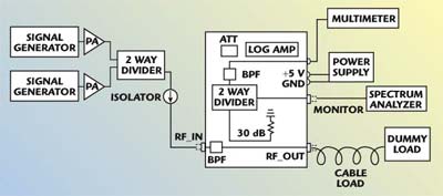
Fig. 1 Diagram of the experimental set-up for RF detection using a logarithmic amplifier.
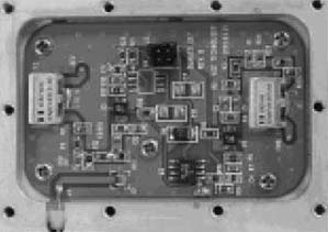
Fig. 2 The RF power detector manufactured with a logarithmic amplifier.
Test Results
To determine the linear dynamic range of this work, the output voltage of the detector as a function of input RF power was measured, as shown in Figure 3. The reference voltage of this detector was 0.755 V and the slope was 0.03 V/dB. In Figure 4, CDMA carriers with the same total power, 25 dBm, were applied to the RF detector and there was no frequency separation between them. As the number of CDMA carriers was increased, the output voltage increased. The voltage difference between one carrier and five carriers was 0.022 V.

Fig. 3 Detector output voltage as a function of input power.
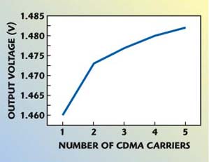
Fig. 4 Power detector output voltage as a function of the number of CDMA carriers.
When two CDMA carriers with different frequency spacing are applied, the resulting output voltage of the detector is shown in Figure 5. When the total power of the two CDMA carriers was 25 dBm, the detected voltage for two CDMA carriers was higher by 0.014 V than for a single CDMA carrier with the same RF power. As the channel spacing was increased, the output voltage of the detector decreased. When the output voltage is normalized to the output with 1 MHz space, the error rate is increased by 1.3 percent. If the output voltage is normalized to the output for one CDMA carrier, the offset voltage is also decreased. However, when the channel space is close to 10 MHz, the slope of change in the offset voltage is much decreased. The maximum voltage difference over 10 MHz is 0.02 V. At this point, the difference in power level can be calculated at a rate of 0.03 V/dB. When two CDMA channels were located with some frequency separation, the maximum voltage was increased by 46 percent compared with the slope of the detector. The rate of difference in detection voltage over 10 MHz was limited to 67 percent. Therefore, the calculated RF power measured through the power detector should be compensated by a maximum of 0.7 dB, compared with that of a single CDMA carrier.
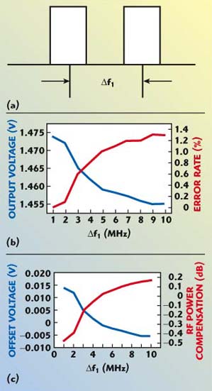
Fig. 5 Experimental results for two CDMA carriers; (a) frequency separation between carriers, (b) detector output voltage as a function of Δf1, and (c) offset voltage and RF compensation compared to a single CDMA carrier.
In a similar manner, the experimental results for three CDMA carriers with different frequency spacings are shown in Figure 6. When the separation between the first and second carriers is Δf1 and the separation between the second and third carriers is Δf2, the detection voltage for three CDMA carriers was higher by 0.018 V than for a single CDMA carrier with the same power. Also, this value was higher by 0.04 V compared with that of two CDMA tones. As Δf1 and Δf2 increased, the detection voltage was decreased. The decrease for three CDMA carriers, as a function of frequency spacing, was similar to that for two CDMA carriers. When three CDMA channels were spaced by some frequency, the maximum voltage was shifted higher by 60 percent compared with the slope of the detector. However, the offset voltage for three CDMA carriers was the same as that for two CDMA carriers when the frequency separation was more than 10 MHz.
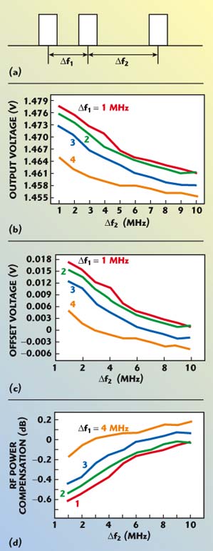
Fig. 6 Experimental results for three CDMA carriers; (a) frequency separation between carriers, (b) output voltage of the detector, (c) offset voltage as a function of frequency separations compared to a single carrier, and (d) RF compensation as a function of frequency separations compared to a single carrier.
In this article, the effect of multi-channel RF signals, in the Korea PCS band, detected with a logarithmic amplifier, is reported. When two CDMA carriers are applied, the detected voltage was higher by 0.014 V compared with the detected voltage for a single CDMA carrier, but decreased as the channel spacing increased. The difference in detected voltage between the 1 MHz and the 10 MHz separation was approximately 0.02 V with respect to a slope of the logarithmic amplifier of 0.03 V/dB; the maximum error in RF power detection was 0.65 dB. In the experiments with three CDMA carriers, the detected voltage was higher by 0.0 18 V compared with the detected voltage of a single CDMA carrier; however, it was decreased in the same manner as in the case of two CDMA carriers.
Conclusion
When the RF powers for multi-carriers are detected, the experiments show that there are offset voltages according to the frequency spacings. Even though the transmitted power is the same, as the number of signals is increasing, the detected voltage increases. However, as the frequency spacing becomes wider, the detected voltage of multi-carriers decreases. When the channel spacing is larger than 5 MHz, the effective detected voltage for CDMA multi-carriers shows a vertical shift in the transfer function. However, the slope of the detected voltage as a function of channel spacing is not affected. For the accurate power-control of CDMA power amplifiers, a compensated, offset voltage should be used.
References
- S.N. Rubin, “A Wideband UHF Logarithmic Amplifier,” IEEE Journal of Solid-state Circuits, Vol. 1, No. 2, December 1966.
- W. Gordon, “Design of a Power Detector for Digital Wireless Amplitude Leveling and Fault Monitoring,” Applied Microwave & Wireless, September 2000, pp. 86–92.
- C. Lodstrom, “The LogProbe Logarithmic Detector,” Applied Microwave & Wireless, December 1999, pp. 72–80.
- Application Notes on 100 MHz–2500 MHz 45 dB RF Detector/Controller, Analog Devices, Norwood, MA 1999.
- E. Nash, “Design a Logamp RF Pulse Detector,” Microwaves & RF, January 2000.
- P. Piro, “Directional Detector Chip Monitors Wireless Handsets,” Microwaves & RF, February 2000.