
The direct conversion, all digital gain control (DC-ADGC) radio receiver employs logarithmic amplifiers in the analog baseband to compress the signal dynamic range before the analog-to-digital converter. An antilog function may then be used in the digital baseband to decompress the signal. Two implementations of the DC-ADGC receiver are considered. The first omits the antilog function and is referred to as the reduced complexity DC-ADGC receiver.
The second, shown in Figure 1, includes the antilog function and is referred to as the enhanced performance DC-ADGC receiver. A traditional direct conversion AGC receiver, which provides a benchmark for performance comparisons, is shown in Figure 2. It will be referred to as the benchmark receiver.

Fig. 1 Direct conversion, all digital gain control receiver.ultipath signals (direct and reflected).

Fig. 2 Benchmark direct conversion AGC receiver.
The following assumptions are made when comparing the DC-ADGC receiver with the benchmark receiver: all receivers under consideration employ the same front-end (low noise amplifier and downconverter); all receiver front-ends have to meet the same noise figure, IP2 and IP3 requirements. These requirements are derived from the 3GPP UTRA/FDD standards1 and are presented in Table 1. In computing the various receiver requirements the following assumptions are made:2 the data processing gain Gp = 10log10 (3.84 Mcps/12.2 kbps) ~ 25 dB; the minimum required signal-to-noise and interference ratio Eb/Nt = 7 dB. All receivers under consideration employ the same number of bits in the analog-to-digital converter.

Both the benchmark receiver and the reduced complexity DC-ADGC receiver employ the same digital root raised cosine (RRC) filter. Inclusion of the digital antilog function requires subsequent sections of the enhanced performance DC-ADGC receiver digital back-end to carry more bits. Therefore, the same RRC filter cannot be used in the enhanced performance DC-ADGC receiver. However, both implementations of the RRC filter are assumed to provide the same ultimate rejection.
All receivers under consideration employ a fully differential analog baseband. In the ideal case, the baseband circuitry does not generate any even-order harmonics. However, odd-order harmonics still need to be considered; therefore, the IP3 of the respective baseband sections are examined.
DC-ADGC Receiver Theory of Operation
The back-end of the DC-ADGC receiver chain, with the digital gain control mechanism, is shown in Figure 3. The DC-ADGC receiver back-end consists of a logarithmic amplifier, an analog-to-digital converter, a digital antilog function, a RRC filter and a normalizer. The normalizer supplies an average output level that remains constant over time to the subsequent sections of the receiver chain. It accomplishes this by first measuring the input signal power and then scaling the input according to a predetermined output level.

Fig. 3 The DC-ADGC receiver gain control mechanism.
The spurious free dynamic range, (SFDR), defined in terms of the input third-order intercept point (IIP3) and noise figure, is a widely used measure of a receiver available dynamic range. In order to determine the instantaneous input third-order intercept point of the back-end, only the chain shown in Figure 4 is considered.

Fig. 4 The DC-ADGC receiver back-end IP3 derivation.
It is expected that the addition of the digital antilog function in the receiver chain will improve the IIP3 of the back-end by a predictable constant amount at each input power level. For simplicity the logarithmic amplifier and the data converter are assumed ideal, and all sources of gain and offset error are applied to points A and B. In order to derive the IP3 of the back-end, xA must be expanded in polynomial form. Then the linear gain and third-order terms of this expansion will be used to determine the instantaneous IP3. Note that A and B are shown to be constants, whereas in a real circuit both will vary with the input signal level, x. It is assumed that the input signal range may be divided into a finite number of small enough sections within which A and B remain constant. Under these circumstances the effect of B is to multiply xA by a constant scaling factor. For the sake of simplicity B is set to zero and A is treated as a constant in the following analysis.
(1–r)< A < (1 + r)
where
|r| < 1
The quantity |A–1| signifies the percentage mismatch (MM%) between the logarithmic amplifier transfer function and the digital antilog transfer function at each input power level. The Taylor expansion of xA about the point x0 is given as

After taking the first four derivatives of xA, inserting them into Equation 1 and simplifying, the following expansion is obtained

The IIP3 of a circuit is defined as the input level at which the third-order IMD terms equal the linear gain term.3 This level is found by letting x equal the sum of two sinusoids with distinct frequencies in Equation 2. Then all linear gain and third-order IMD terms that result are collected and the input level at which they are equal is found as
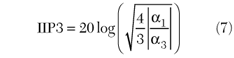
If the quantity A is sufficiently close to unity, the expressions for a1 and a3 given in Equations 4 and 6 simplify considerably and as a result Equation 7 may be expanded and simplified to

Note that the simplified DC-ADGC receiver back-end input IP3 (IIP3est) expression listed above is a function of the input power. The final IP3 of the receiver will be a combination of the front-end and the back-end IP3s. If the first two terms in the expression are assumed to be a specification of the instantaneous IIP3 of the back-end without the antilog function, then the expression may be rewritten in the following form

Equation 8 reveals that the amount of back-end IIP3 improvement due to the addition of an antilog function is equal to 10 times the logarithm of the log to antilog mismatch at each input power level. If the log-antilog mismatch percentage, |A-1|, remains constant throughout the input signal range, the IIP3 curves of the back-end with and without the antilog function given in Equations 8 and 9, respectively, will be parallel straight lines when plotted on a log-log scale.
In Figure 5, the two parallel lines represent the predicted instantaneous IIP3 of the DC-ADGC receiver without the digital antilog function and the improvement due to the addition of a 10 percent matched antilog function as predicted by Equation 8. The measured back-end instantaneous IIP3 with and without the digital antilog function are also plotted. The experimental data closely follows the predicted IIP3 curves for higher input signal levels. For relatively low signal levels the practical logarithmic amplifier generates little or no distortion. Therefore, the improvement in IIP3 due to the inclusion of the antilog function is noticeable only at higher signal levels.

Fig. 5 The DC-ADGC receiver back-end IIP3.
The available dynamic range of a receiver is a function of the input linearity and sensitivity of the receiver. The SFDR defined in terms of the input third-order intercept point and noise figure is a widely used measure of a receiver available dynamic range3

where
IIP3 = Receiver cascaded input third-order intercept point
NF = Receiver cascaded noise figure
BW = Noise bandwidth of the system
KT = –174 dBm/Hz
In computing the cascaded noise figure and the cascaded input third-order intercept point, consider the block diagram in Figure 6. The three blocks in the simplified receiver chain are the front-end, the gain block and the back-end. The gain block between the front-end and the back-end is necessary to meet the overall receiver noise figure (< 9 dB) specification. Figure 7 illustrates the spurious free dynamic range of the DC-ADGC receiver.

Fig. 6 Simplified DC-ADGC receiver chain.
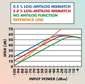
Fig. 7 The DC-ADGC receiver spurious free dynamic range.
As an illustration, the SFDR curves of two possible grades of the enhanced performance DC-ADGC receiver and that of the reduced complexity DC-ADGC receiver are plotted. The yellow line is a reference line of unity slope, which represents the SFDR of an ideal receiver. Note that if the SFDR curves are kept to the left of the reference line over the entire input range, then all in-band spurs created by interferers of any power level within the input range will remain below the desired signal level. The remaining three curves represent the SFDR curves of a DC-ADGC receiver without an antilog function and DC-ADGC receivers with 0.5 and 5 percent mismatched antilog functions.
Consider the enhanced performance DC-ADGC receiver with a 5 percent mismatched antilog function. At an input level of –52 dBm, the spurious free dynamic range is 41 dB. The UTRA/FDD standards’ adjacent channel selectivity test calls for an input signal power of –103 dBm and an adjacent channel CDMA modulated interferer power of –52 dBm.1 The in-band spurs created by the DC-ADGC receiver under consideration will be at –93 dBm. Therefore, all but 10 dB of the required 33 dB adjacent channel selectivity may be placed in the digital baseband RRC filter. Note that the 10 dB analog selectivity requirement is based on a 5 percent mismatched antilog function. If, for example, the implemented antilog function were 10 percent mismatched, the back-end IIP3 would be 3 dB lower. Therefore, the resulting SFDR at the –52 dBm input power level would be 39 dB and the required analog selectivity would be 12 dB.
Another approach to determining the amount of analog selectivity enhancement possible through digital filtering is to examine the receiver error vector magnitude (EVM) in the presence of adjacent channel interferers. Test data collected from the implemented reduced complexity and enhanced performance DC-ADGC receivers is presented in Figure 8. The test was conducted with a linear-phase, low pass filter in the receiver analog baseband, which provided no more than 6 dB of adjacent channel selectivity. The primary purpose of the filter was to limit the amount of noise appearing at the logarithmic amplifier input. The 1-code forward link FDD-WCDMA signal on the desired channel was fixed at a certain power level, while the 2-code FDD-WCDMA adjacent channel interferer (jammer) was power swept relative to the wanted signal.

Fig. 8 The DC-ADGC receiver EVM vs. interferer power, relative to signal power.
As an illustration, limit the allowable receiver EVM to 18 percent. A jammer, 27 dB above the desired signal, will result in an EVM of 18 percent in the implemented enhanced performance (10 percent mismatched antilog function) DC-ADGC receiver. Note that the receiver must be able to tolerate a jammer that is 33 dB above the desired signal. Therefore, the required adjacent channel analog baseband selectivity is 33 dB –27 dB +6 dB (existing Bessel filter in the analog baseband) = 12 dB. It is clear that the enhanced performance receiver as compared to the reduced complexity DC-ADGC receiver is much more immune to adjacent channel interferers.
A Comparison of the DC-ADGC Receiver and the Benchmark AGC Receiver
Figure 9 is a comparison of the spurious free dynamic ranges of the DC-ADGC receiver and the benchmark direct conversion AGC receiver. The unity slope yellow line represents the SFDR of an ideal receiver. Representative SFDR curves of a DC-ADGC receiver with 0.5 and 5 percent mismatched digital antilog functions are plotted along with the SFDR curves of a benchmark receiver with a high IP3 and a poor IP3 final analog stage.

Fig. 9 SFDR of the DC-ADGC and benchmark receivers.
The overall noise figure of a traditional DC-AGC receiver increases with increasing input signal. This is because the gain of the receiver decreases as the input power increases. Also note that the benchmark receiver SFDR at the minimum input signal level depends largely on the final analog stage IP3. However, as the input signal level increases, the noise figure of the benchmark receiver increases with it and starts to reduce the SFDR. Finally, at high input power levels the SFDR of the benchmark receiver is limited by the front-end IP3. In contrast, the SFDR range of the DC-ADGC receiver starts out low at low input signal levels and increases until the back-end IP3, which is a function of the input power level, starts to approach the IP3 of the front-end. Beyond this point, the IP3, and therefore the SFDR of the DC-ADGC receiver, is limited by the front-end IP3. The noise figure of the DC-ADGC receiver remains constant throughout.
In order to gauge the complexity of the DC-ADGC receiver relative to the benchmark direct conversion AGC receiver, consider the gain control schemes employed by each receiver. An illustration of the DC-ADGC receiver gain control scheme was shown earlier. The implementation of a typical AGC loop is shown in Figure 10.

Fig. 10 Typical receiver automatic gain control scheme.
In comparison to the simple, open loop level normalization scheme of the DC-ADGC receiver, the benchmark receiver employs a complex closed loop AGC scheme. The two gain control schemes are contrasted in Table 2.

Conclusion
It is predicted that, in advanced mobile communication markets of the future, packet-switched traffic will overtake circuit-switched traffic. It is also predicted that future mobile user applications are likely to involve the transport of large volumes of digital multimedia data that is bursty in nature and requires high bit rates. This ever increasing user demand for data intensive services will drive operators to optimize their networks to support high speed, time multiplexed, asynchronous, packet-switched traffic. High Speed Downlink Packet Access (HSDPA), which is an evolution of WCDMA, standardized as a part of the 3GPP Release 5 WCDMA specification, is already a step in that direction. HSDPA improves system capacity and increases user data rates in the downlink direction. This is anticipated to be the typical scenario where the user requests data, and, in response, the base station quickly downloads large volumes of digital multimedia data in bursts to the user equipment.
Furthermore, the proposed fourth generation (4G) systems will be entirely built on packet-switched networks and will have to support high velocity (250 kph) and high data rate (20 Mbps) traffic. UE receivers in 4G networks will have to operate in very fast fading channels where 6 to 8 dB fades per millisecond will be typical. Therefore, UE receivers of the future will have to be capable of handling large instantaneous variations in received power. Some features of the DC-ADGC receiver, in line with the above requirements and others that are generally attractive from a cost and complexity standpoint, are listed below.
The DC-ADGC receiver provides a large instantaneous dynamic range (> 60 dB) and is therefore capable of handling large instantaneous variations in the received power. This is accomplished by the use of a logarithmic amplifier in the analog baseband section and a fast settling gain normalizer. The receiver also provides SFDR where it is needed in the input signal range, which means enhancement of analog selectivity through digital filtering is possible.
The DC-ADGC receiver employs an all-digital gain control mechanism and does not require analog gain control amplifiers or an AGC feedback loop. This facilitates a reduced receiver component count by eliminating the need for external filter inductors and AGC D/A converters, and does away with the need to provide gain control input pins on the receiver IC.
In conclusion, the DC-ADGC receiver, as compared to the existing user equipment grade direct conversion AGC receiver, better accommodates packet-switched, asynchronous burst data traffic, facilitates high integration and possesses a simpler, lower component count analog section while maintaining or in some cases exceeding the level of performance.
Acknowledgment
The authors gratefully acknowledge the support of Dr. Robert DeFazio, Gerard Klahn and Timothy Axness from InterDigital Communications Corp.
References
- Third Generation Partnership Project (3GPP), “UE Radio Transmission and Reception (FDD),” Technical Specification 25.101, Vol. 3.6.0, 1999.
- O.K. Jensen, T.E. Kolding, C.R. Iversen, S. Laursen, R.V. Reynisson, J.H. Mikkelsen, E. Pedersen, M.B. Jenner and T. Larsen, “RF Receiver Requirements for 3G W-CDMA Mobile Equipment,” Microwave Journal, Vol. 43, No. 2, February 2000, pp. 22–46.
- B. Razavi, RF Microelectronics, Prentice Hall, Upper Saddle River, NJ, 1998.