
Due to the inherent upper limit in operating frequency of active devices in local oscillators, a frequency multiplier, in conjunction with a low frequency local oscillator, has often been used as a signal source, providing better overall phase-noise performance and low cost realization.1 A balanced configuration has been widely used for microwave and millimeter-wave frequency doublers because of its high conversion gain, effective suppression of fundamental and odd harmonic frequencies, as well as high output power.2–5 Fundamental signals are suppressed by out-of-phase cancellation at the output load, while the desired second harmonic components are power combined in-phase in the balanced frequency doubler configuration. In balanced frequency doublers, an input power divider, such as a 90° hybrid or balun, and an output power combiner have typically been used.2–5 In general, however, by utilizing an input power divider, the peak value of the input sinusoidal voltage signal, which is driving a nonlinear device, is reduced by a factor of ?2. This results in a weak device drive and the reduction of the conversion gain.
In this article, a new balanced-like frequency doubler scheme is presented. Its fundamental operation in terms of drain currents is similar to the conventional balanced doubler, hence the name — quasi-balanced frequency doubler. The proposed quasi-balanced frequency doubler scheme is realized, however, by incorporating an alternate input power dividing and output power combining technique. Compared to the operation of an ordinary balanced configuration, the power dividing and combining method maintains the peak value of the driving input sine-wave at a level equal to the source signal level by making use of the properties of FETs biased in class-B. Therefore, this results in a significant enhancement of the conversion gain. A 5 to 10 GHz quasi-balanced frequency doubler has been successfully demonstrated based on this power dividing and combining technique.
Circuit Configuration and Operating Principle
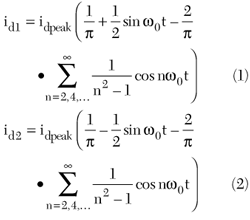
The conventional balanced frequency doubler, with a 180° hybrid, is composed of two anti-symmetrical FET half-wave rectifiers and an input power divider, as depicted in Figure 1.5 IMN@f0 and OMN@2f0 are the input and output-matching networks designed at the fundamental and second harmonic frequencies, respectively. Since the FETs are typically biased in the pinch-off operation region, conduction of the FETs occurs on alternating positive and negative cycles of the driving signal defined as an input signal of the FETs. The connection point A becomes a virtual ground. In fact, Fourier analysis of the current waveform at the drain of each device reveals that they consist of a DC term, a fundamental term and a series of even harmonics, as in Equations 1 and 2. In these equations, it can easily be seen that the fundamental components are 180° out-of-phase while the desired even harmonic components are in-phase, thereby offering ease in the suppression of the unwanted out-of-phase fundamental signal components.
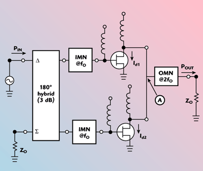
Fig. 1 Schematic of a conventional balanced frequency doubler.
Moreover, it should be noted that the peak voltage at the output of the 180° power divider is lower by a factor of ?2 than that of the source signal, due to the 3 dB input power divider.
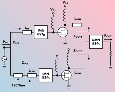
Fig. 2 Circuit diagram of the quasi-balanced frequency doubler.
The proposed quasi-balanced frequency doubler, which is based on the alternate power dividing and combining techniques to maintain the peak voltage value, is shown in Figure 2. Like the conventional balanced structure, this frequency doubler is composed of two anti-symmetrical FET half-wave rectifiers. The basic operating principle, in terms of the conduction, is the same as in Equations 1 and 2. However, in the proposed configuration, neither an external input power divider nor a power combiner was incorporated with the FETs. Instead, a single 180° microstrip line is added to one side of the pair of FETs for differential excitation of the fundamental frequency source signal. By making use of the differential excitations generated by the 180° line and the nature of the FETs biased in class-B, the alternate power dividing and combining techniques used to prevent a decrease of the peak value of source signal is realized. This results in larger magnitude current components in Equations 1 and 2. The fundamental operating principle of the power dividing/combining method and the quasi-balance doubler is as follows:
FET input and output impedances are nearly reactive with a small resistive value when it is biased in the pinch-off region.6–7 When offset microstrip lines, LIN and LOUT, with the correct length are added, these impedances can easily be transformed into high resistive values. Thus, when the upper branch is operating, the input and output impedances ZIN2 and ZOUT2 become high enough for the source signal to be directed into the upper FET by means of the offset lines. As a result, the positive half-wave cycles are driven only to the upper FET and the signal passes through the upper branch. Likewise, the negative cycles are fed to the FET in the lower branch. Combination of the output currents results in summing the desired second harmonic power and eliminating the fundamental frequency components.
Circuit Design
The circuit operation described in the previous section was applied to the design of a 5 to 10 GHz quasi-balanced frequency doubler. The Agilent ADS’s harmonic balance simulator and a packaged 280 mm-wide NEC 76038 GaAs FET nonlinear model were utilized in the simulation. The design was accomplished using the following procedures: As a first step, the optimum output impedance at the 10 GHz second harmonic frequency for maximum output power from the GaAs FET biased in class-B configuration was extracted using load-pull simulation. The input power level was set to 1 dBm, with a corresponding 1 dB backoff in the linear second harmonic power characteristic.
A single-ended frequency doubler that forms one branch of the quasi-balanced circuit was designed. The output impedance was matched to the extracted impedance at 10 GHz and the input matching was done at 5 GHz. To improve the conversion gain of the single-ended circuit, a second harmonic frequency reflector was added in the input matching side.8–10 Since the device nonlinearities cause many frequency components to be mixed, the desired signal may be enhanced or degraded depending upon the phase. A simple LC-tank type resonator designed at 5 GHz was used in the simulation to optimize the desired second harmonic input impedance for maximum conversion gain.10 The resonator tunes the 10 GHz input impedance as well as reflects the 10 GHz back with no effect on the 5 GHz impedance. In practice, due to the difficulty in realizing the LC-tank circuit at microwave frequencies, the resonator was implemented through the use of a parallel-coupled stripline stepped impedance resonator.11 Note that the impedance values were equal for the two resonators at 5 and 10 GHz so that the same simulation results remain. The offset microstrip line at the output side, LOUT, was added as part of an output-matching network in order to obtain ZOUT1 or ZOUT2 of high impedance value when the corresponding FET is driven beyond pinch-off. Two of these structures were combined using an input offset line, LIN, serving the same purpose as LOUT at the output, and a 180° line for differential excitation.
Figure 3 shows the simulated large-signal performance. The simulated 10 GHz output power is shown as a function of the 5 GHz input signal for the quasi-balanced doubler and compared to the simulated output power of the conventional balanced-type frequency doubler. Note that all design parameters, such as FETs and bias conditions for the conventional doubler were the same as for the quasi-balanced circuit.
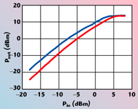
Fig. 3 Simulated output power of the conventional (red) and quasi-balanced (blue) frequency doublers.
As clearly shown, the proposed quasi-balanced doubler provides a higher conversion gain than the conventional doubler. This is because of the alternate power dividing and combining technique, which enables the peak value of the driving voltage to be larger than in the conventional doubler case. Since the FETs used are identical for both doublers, the saturated output power levels are almost the same in the high input power range.
Measurement Results and Discussions
The designed single-ended and quasi-balanced frequency doublers were fabricated on a 0.787 mm thick RT/Duroid substrate with a dielectric constant of 2.33. The photographs of both circuits are shown in Figure 4. As shown, the single-ended circuit is identical to one branch of the quasi-balanced frequency doubler. Two single-ended doublers were combined together in the quasi-balanced doubler. The input 180° line was added to the upper branch.
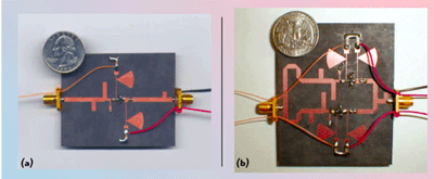
Fig. 4 The fabricated frequency doublers; (a) single-ended and (b) quasi-balanced.
For testing the large-signal performance of the two frequency doublers, the bias voltages were set to VDS = 3 V and VGS = –0.8 V, for class-B operation. First, the single-ended doubler was tested with an input frequency of 5 GHz. Figure 5 shows the measured output power at 10 GHz and the conversion gain as a function of input power. An output power of 7.3 dBm was measured for 1 dBm input power, which was the same power level as in the ADS simulation. A 6.3 dB conversion gain was obtained from the single-ended frequency doubler.
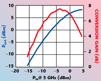
Fig. 5 Measured Pout and conversion gain of the single-ended frequency doubler.
The same bias voltages were applied for the quasi-balanced frequency doubler structure. The measured output power and conversion gain are shown in Figure 6 as a function of the input power.
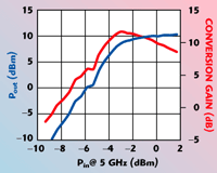
Fig. 6 Measured Pout and conversion gain of the quasi-balanced frequency doubler.
At 1 dBm input power level, an output power of 10.17 dBm was obtained so that the conversion gain became 9.17 dB. By alternately selecting each branch depending on the polarity of the input signal, without equal splitting of the input power between the two branches, a 2.87 dB improvement in the conversion gain and output power was achieved, relative to the measured data of the single-ended structure. Ideally, a 3 dB improvement can be obtained provided the input and output impedances of one branch are infinite when the other branch is conducting. In practice, however, the improvement becomes smaller than 3 dB. This is because the finite impedance values cause a loading effect from one branch to the other.
Figure 7 shows the measured output power and conversion gain over the frequency range from 9.94 to 10.1 GHz. The input power for this measurement was set to 1 dBm.
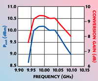
Fig. 7 Measured frequency dependence of Pout and conversion gain of the quasi-balanced frequency doubler.
At frequencies close to the designed 10 GHz, a 9.5 dB conversion gain and 10.2 dBm output power was observed. However, as frequency departs from the designed 10 GHz the conversion gain and output power decrease significantly. This narrow bandwidth characteristic is caused by both the frequency-dependent 180° microstrip line at 5 GHz for the differential excitation at the input side, and the input and output impedance transformation by the offset lines. The bandwidth of the quasi-balanced scheme can be improved by employing a wide-band circuit for providing differential inputs.
The measured phase-noise performance (single sideband carrier to noise ratio) of the quasi-balanced frequency doubler is shown in Figure 8 over an offset frequency range from 1 kHz to 1 MHz. The input power at 5 GHz was set to 1 dBm for this measurement. At a 100 kHz offset frequency, a –110 dBc/Hz phase-noise was obtained, achieving –129 dBc/Hz at a 1 MHz offset. Compared to the phase-noise of the synthesizer used as an input signal source, the phase-noise of the quasi-balanced doubler is approximately 5 dB higher over the entire measured offset frequency range.
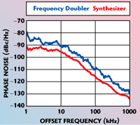
Fig. 8 Measured phase-noise performance of the quasi-balanced frequency doubler.
In this quasi-balanced circuit configuration, the 180° delay line on one side of the two FETs provides the differential excitations for the 5 GHz fundamental input signal. As described in the previous section, the out-of-phase fundamental frequency signal can be effectively eliminated in the same fashion as in a conventional structure by combining two branches at the output matching side. The measured suppression characteristics for the fundamental 5 GHz frequency and 15 GHz third-harmonic frequencies with respect to the input power in the range from –10 to 2 dBm are shown in Figure 9.
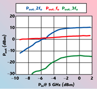
Fig. 9 Measured suppression characteristics of the quasi-balanced frequency doubler.
Relative to the 10 GHz frequency signal, the suppression was –7.16 dBc at 5 GHz and –25 dBc at 15 GHz. The measured suppression characteristic results were not as low as the simulation results that show –50 dBc for the fundamental frequency using a FET nonlinear model in ADS simulation. This discrepancy may be caused by the mismatches between the two operating branches. Imperfections in the implementation of hybrid microwave circuits and an inaccurate transistor model, especially in the pinch-off region, may also contribute to the degradation of the suppression characteristic. The suppression may be enhanced by accurately controlling the phase delay at the fundamental frequency and improving the transistor nonlinear model biased in class-B configuration.
Conclusion
A new quasi-balanced frequency doubler has been developed using an alternate power dividing and combining technique. The technique enables the either positive or negative excursion of the source signal to be directed into FETs alternately depending on the polarities of the source signal. This allows a larger driving signal level for each FET, thereby increasing the output power and enhancing the frequency conversion gain. The operating principle is based on the nature of FETs biased into the pinch-off operating region. In the quasi-balanced configuration, the conversion gain and output power have been improved by up to 3 dB more than that of a single-ended structure by feeding the input signal in the proposed manner. A 9.17 dB conversion gain and 10.17 dBm output power were obtained for the successfully demonstrated 5 to 10 GHz doubler configuration, which is a 2.87 dB improvement in the conversion gain and output power relative to the measured performance of the single-ended schemes.
References
1. M. Funabashi, T. Inoue, K. Ohata, K. Maruhashi, K. Hosoya, M. Kuzuhara, K. Kanakawa and Y. Kobayashi, “A 60 GHz MMIC Stabilized Frequency Source Composed of a 30 GHz DRO and a Doubler,” 1995 IEEE International Microwave Symposium Digest, pp. 71–74.
2. A. Yanev, B.N. Todorov and V. Ranev, “A Broadband Balanced HEMT Frequency Doubler in Uniplanar Technology,” IEEE Transactions on Microwave Theory and Techniques, Vol. 46, No. 12, December 1998, pp. 2032–2035.
3. Y. Campos-Roca, L. Verweyen, M. Fernándes-Barciela, W. Bischof, M.C. Currás-Fransco, E. Sánchez, A. Hülsmann and M. Schlechtweg, “38/76 GHz PHEMT MMIC Balanced Frequency Doublers in Coplanar Technology,” IEEE Microwave and Guided Wave Letters, Vol. 10, No 11, November 2000, pp. 484–486.
4. I. Angelov, H. Zirath, N. Rorsman and H. Grönqvist, “A Balanced Millimeter-wave Doubler Based on Pseudomorphic HEMTs,” 1992 IEEE International Microwave Symposium Digest, pp. 353–356.
5. E. Camargo, Design of FET Frequency Multipliers and Harmonic Oscillators, Artech House Inc., Norwood, MA, 1982.
6. S. Yanagawa, H. Ishihara and M. Ohtomo, “Analytical Method for Determining Equivalent Circuit Parameters of GaAs FETs,” IEEE Transactions on Microwave Theory and Techniques, Vol. 44, No. 10, October 1996, pp. 1637–1641.
7. B.L. Ooi, P.S. Kooi and M.S. Leong, “A New Pinched-off Cold FET Model for the Determination of Small-signal Equivalent Circuit of a FET,” Proceedings of the Asia-Pacific Microwave Conference, 1997, pp. 713–716.
8. Y. Iyama, A. Iida, T. Takagi and S. Urasaki, “Second-harmonic Reflector Type High Gain FET Frequency Doubler Operating in K-band,” 1989 IEEE International Microwave Symposium Digest, pp. 1291–1294.
9. D.G. Thomas, Jr. and G.R. Branner, “Single-ended HEMT Multiplier Design Using Reflector Networks,” IEEE Transactions on Microwave Theory and Techniques, Vol. 49, No. 5, May 2001, pp. 990–993.
10. Y. Chung, D Ahn and T. Itoh, “Optimization of Second Harmonic Input Impedance for High Conversion Gain Frequency Doubler,” Proceedings of the Asia-Pacific Microwave Conference, Vol. 3, 2003, pp. 1668–1671.
11. M. Makimoto and S. Yamashita, “Bandpass Filters Using Parallel Coupled Stripline Stepped Impedance Resonators,” IEEE Transactions on Microwave Theory and Techniques, Vol. 28, No. 12, December 1980, pp. 1413–1417.
Younkyu Chung received his PhD degree in electrical engineering from the University of California at Los Angeles in 2004. In March 2004 he joined the Center for the Physics of Information at the California Institute of Technology, where he is a post-doctoral scholar working on millimeter-wave amplifiers and frequency multipliers. His current research focus is on the design of microwave/millimeter-wave amplifiers and frequency multipliers, combining techniques and advanced RF front-ends. He was the recipient of the IEEE Microwave Theory and Techniques Society graduate student fellowship in 2002 and a Caltech post-doctoral research fellowship in 2004.
Dal Ahn received his BS, MS and PhD degrees in electronics from Sogang University, Seoul, Korea, in 1984, 1986 and 1990, respectively. In 1992 he joined the School of Electrical and Electronic Engineering, Soonchunhyang University, Asan, Korea, where he is currently a professor. He is also currently the chief of the RF and microwave component research center (RAMREC), Soonchunhyang University, Asan, Korea. His research interests include the design and application of passive and active components at radio and microwave frequencies, circuit modeling using commercial electromagnetic analysis programs, and defected ground structure (DGS) applications for RF and microwave components.
Tatsuo Itoh received his PhD degree in electrical engineering from the University of Illinois, Urbana, IL, in 1969. He has held teaching positions at the University of Illinois, SRI, University of Kentucky, AEG Telefunken in Germany and the University of Texas at Austin. In January 1991 he joined the University of California at Los Angeles as a professor of electrical engineering and holder of the TRW Endowed Chair in Microwave and Millimeter-wave Electronics. He has received numerous awards, including the Shida Award from the Ministry of Post and Telecommunications, Japan, the Japan Microwave Prize, the IEEE Third Millennium Medal and the IEEE Distinguished Educator Award. His work has appeared in over 1000 publications in the areas of microwave and millimeter-waves, computational electromagnetics, antennas, microwave photonics, EBG, and negative index materials.