

The advancement of semiconductor technologies is driving the emergence of new and expanded applications within the mmWave and sub-THz frequency spectrums. These applications include 5G, 6G and upcoming evolutions of wireless communications, radar in automotive and security markets, imaging and sensing, radio astronomy, satellite communications, military applications like electronic warfare and scientific research. Whether a particular semiconductor technology is ultimately successful in one or more of these applications is determined, in part, by its performance in certain critical areas, including output power, gain and efficiency. Designers can determine and optimize these performance parameters through device characterization and, more specifically, by performing power sweep and load-pull measurements.
AN INTRODUCTION TO LOAD-PULL MEASUREMENTS
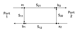
Figure 1 Two-port network representation of DUT.
Load-pull refers to the technique of altering the load impedance presented to a device under test (DUT), typically a transistor. This is done to assess the performance characteristics of the device across different large signal conditions. Systematic adjustments are made to impedances while concurrently measuring or calculating parameters like output power, gain and efficiency. Contours are generated to reflect fixed performance values, such as an output power of X dBm or efficiency of Y percent. These contours aid in visualizing the optimum performance point, understanding how performance changes and evaluating the trade-offs between different parameters.
To understand the load-pull technique, consider a DUT as a two-port network, as shown in Figure 1. The magnitude of reflection, ΓL, is calculated as shown in Equation 1:

Load-pull changes the magnitude of reflection presented to the load of the DUT by manipulating the reflected signal, a2, and this manipulation has a similar effect on the phase of the reflection signal. Any load impedance can be expressed as the relationship shown in Equation 2.

This relationship can be applied to the DUT as long as achieving the desired a2 signal is feasible.
There are two common methodologies to vary the impedance presented to a DUT: passive load-pull and active load-pull. Passive load-pull employs mechanical impedance tuners to modify both the magnitude and phase of a2, which alters the impedance encountered by the DUT. Instead of using a mechanical tuner, active load-pull artificially creates, controls and injects the a2 wave into the output port of the DUT to synthesize the desired ΓL condition. In the specific case of open loop active load-pull, an external signal source that is phase-coherent with the a1 wave and equipped with magnitude and phase control is used to generate a2.
OPEN LOOP ACTIVE LOAD-PULL AT MmWAVE AND SUB-THZ FREQUENCIES
Armed with these basic concepts, the block diagram of a typical mmWave and sub-THz active load-pull system is shown in Figure 2. The system works by generating an RF signal using the first signal source embedded in the vector network analyzer (VNA). The RF signal is routed into the vector modulator unit (VMU) where it is split into an RF1 and an RF2 signal that can be independently manipulated in magnitude and phase using embedded IQ modulators. The RF1 signal is routed into the VNA frequency extender module at the input of the DUT and the RF2 signal is routed into the VNA extender on the output side of the DUT. The VNA extender modules provide frequency up-conversion for the RF signals with an extender-specific frequency multiplication factor that takes the signals to the mmWave or sub-THz frequency of interest. The up-converted RF1 signal, which is equivalent to the a1 wave shown in Figure 1, is injected into the input of the DUT to drive it at a specific power level. The up-converted RF2 signal, which is equivalent to the a2 wave shown in Figure 1, is injected into the output of the DUT. By using the VNA extender modules to measure the b2 wave, it is possible to iteratively adjust the injected a1 wave to obtain the desired load condition. The drive power for the DUT is dependent on the power output of the VNA extender module, minus any losses between the module and DUT. An example of these losses would be losses caused by the wafer probe. It is important to note that the RF1 and RF2 signals, and therefore the a1 and a2 waves, are phase-coherent since they have been generated from the same signal source within the VNA. Additionally, the b2 wave will be phase-coherent with the a1 wave and with the a2 wave. This allows the a2 wave to be properly adjusted with respect to the b2 wave to obtain the desired ΓL response.
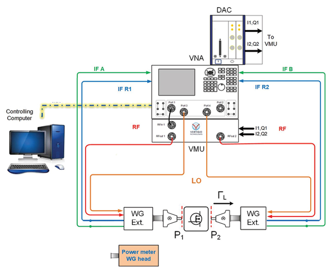
Figure 2 mmWave and sub-THz active load-pull system block diagram.
The formula that governs the relationship between the transistor, the system impedance, the injection power and the tuning range is presented in Equation 3:

Where:
ZL is the impedance presented to the DUT
ZSys is the system impedance
ZDUT is the DUT’s output impedance
The factor K is defined in Equation 4:

Where:
Pa2 is the active tuning power injected into the output of the DUT at the DUT reference plane
Pb2 is the DUT’s output power
Z0 = 50 Ω
The net magnitude of reflection achievable at the DUT reference plane can be calculated using the equation shown in Equation 5:

From Equation 5, a higher available output power, Pa2, allows for a higher achievable ΓL or Smith chart coverage. In a mmWave and sub-THz active load-pull system, the available power is determined by the VNA extender module used to up-convert the signal to mmWave or sub-THz frequencies.