
Technical Feature
A Feedforward Power Amplifier with Loops to Reduce RX Band Noise and Intermodulation Distortion
This article proposes a new power amplifier approach for the reduction of amplified noise signals in the receiver (RX) band as well as intermodulation distortion signals in the transmitter (TX) band using a feedforward technique. The proposed power amplifier, which contains two loops, the TX band intermodulation distortion cancellation loop and the RX band noise cancellation loop, can provide a duplexer with low transmit path insertion loss by choosing a small receive attenuation characteristic. A two-tone test for the power amplifier is done at 2.14 GHz with a frequency spacing of 5 MHz. A 31 dB reduction for the intermodulation distortion signals is obtained. Experimental loop tests show that the cancellation performance of TX band intermodulation distortion signals and RX band noise signals are more than 26 dB and 30 dB over the entire TX and RX bands, respectively.
Yong-Chae Jeong
Division of Electronic and Information Engineering
Chonbuk National University
Chonju, Korea
In communication systems, it is important to isolate undesired signals from desired signals for good voice and data transmission. In code division multiplex access (CDMA) systems, the amplified transmitter signals must be directed through to the antenna and not to the receiver path. Since amplified transmitter signals can appear as noise in the receiver signals, the cost of the RF front-end section is influenced mainly by the isolation characteristics between the TX and RX paths signals.
|
|
|
Fig. 1 Signal flow in a full duplexing communication system. |

When amplifying TX band signals, RX band noise signals are also amplified and transferred to the duplexer without attenuation, as shown in Figure 1 , while some of them are directed into the RX path. Thus, the RX band signal-to-noise ratio (SNR) is decreased. To improve the isolation characteristic to the RX path, the RX band attenuation of the TX bandpass filter should be increased, which also increases the TX path insertion loss. To compensate for the increased TX path insertion loss, the output power of the TX amplifier should be increased. As the output power increases, the cost of the power amplifier is also increased. Consequently, an increase in the isolation characteristics between transmitter and receiver results in higher system costs.
In the case of a TX power amplifier, intermodulation distortion signals are present when TX signals are amplified. Several methods to cancel intermodulation distortion signals have been proposed.1-9 The feedforward linearization method has been a popular technique for reducing distortion at the output of multi-carrier cellular basestations. Ideally, the distortion signals should be cancelled completely over an unlimited bandwidth. However, the practical difficulties of accurately matching phase, amplitude and delay impose limits, especially since the input and output impedance values for optimum high power matching of transistors are very small. As a result, the impedance matching to the characteristic impedance (50 W) can only be realized over a narrow band. Consequently, it is very difficult to realize a feedforward type wideband linear power amplifier for high power levels.10
This article proposes a new feedforward power amplifier with two loops, a TX band intermodulation distortion cancellation loop and RX band noise cancellation loop, to reduce the intermodulation distortion signals and to improve the RX rejection characteristic. The RX band noise cancellation loop, which has an RX bandpass filter to reject the TX signals, is very similar to the loop configuration for the feedforward technique. By adding the RX band cancellation loop, even though the TX band intermodulation distortion cancellation loop has a narrow bandwidth, the RX band noise signals can be reduced significantly in the TX output.
|
|
|
Fig. 2 Block diagram of the proposed power amplifier. |

The Proposed Power Amplifier's Block Diagram and Operation
The block diagram of the proposed power amplifier is shown in Figure 2 . The operation of the proposed amplifier is well illustrated with four-tones spectra that are represented in Figure 3 . The input signals, shown in Figure 3a, consist of two-tone TX signals and RX noise signals. These signals are divided by coupler 1 into a main- and a sub-path. When the signals injected into the main path go through the main amplifier, intermodulation distortion signals are generated at the output of the main amplifier (point A, shown in Figure 3b). Parts of these signals are extracted at the output of the main amplifier by a directional coupler. The extracted signals are injected into a subtracter in the TX intermodulation distortion cancellation loop and in the RX bandpass filter in the RX noise cancellation loop through a Wilkinson divider. The other signals injected into the subtracter are shown in Figure 3c, and only the intermodulation distortion signals are present at subtracter output (point B), as shown in Figure 3d. The conditions for the cancellation of the intermodulation signals are the magnitude of the signals which are injected into coupler 3 via the TX intermodulation distortion cancellation loop, and must have the same magnitude as the intermodulation distortion signals, which are injected through the delay line. In addition, the phase difference between the signals which are injected into coupler 3 via the TX distortion cancellation loop and the intermodulation distortion signals which are injected through delay line must be 180°. The intermodulation distortion signals at the subtracter output are adjusted to satisfy these conditions by a variable attenuator (A2 ), a phase shifter (f2 ) and an error amplifier 1.
|
|
|
Fig. 3 Frequency spectra at different points in the amplifier's block diagram. |

When both conditions are satisfied, the intermodulation distortion signals are eliminated at the output of coupler 3 (point C), as shown in Figure 3e. The cancellation limitations are given as a function of the phase and amplitude errors, as3
Cancellation (dB) = 10 log ësin2 fe + (1-cos fe )2 û (1)
Cancellation (dB) = 20 log [|10E/20 - 1|] (2)
where
fe and E = phase error (degrees) and the amplitude error (dB) between the two paths
However, the RX noise signals are still not eliminated because of the limited frequency properties of the circuits in the TX intermodulation distortion cancellation loop. These results were also obtained with conventional feedforward power amplifiers. The amplified RX noise signals are transferred to the duplexer without attenuation, thus decreasing the system performance.
In this article, an additional cancellation loop is used to eliminate the RX noise signals. The RX bandpass filter is designed to extract only the RX noise signals in this loop, and the spectrum at the RX bandpass filter output (point D) is shown in Figure 3f. This RX bandpass filter can be replaced by a TX band-rejection filter. Similar to the operation of the TX intermodulation distortion cancellation loop, the RX noise signals through the RX bandpass filter are adjusted by a variable attenuator (A3 ), a phase shifter (f3 ) and an error amplifier 2. Figure 3g shows the final output signals where the RX band noise signals are eliminated. The delay time of the RX band noise signals passing through the RX bandpass filter, variable attenuator (A3 ), phase shifter (f3 ) and error amplifier 2 is compensated with the main path delay line. The main delay line that is connected at the main amplifier output port is not only used to compensate the delay time of the TX intermodulation cancellation loop, but also used to compensate the delay time of the RX noise cancellation loop. Since the noise signals level is very low, the error amplifier 2 requires only a very small power output. Since coupler 4 has a low coupling coefficient, the reduction in the TX signals level can be ignored.
Detailed Circuit Design
|
|
|
Fig. 4 Characteristics of the main amplifier. |
The implemented main amplifier consists of an ERA-5SM, a XHL-21336 and a MRF-19030 amplifier, and has a gain of 57 dB with a flatness of 0.24 dB over the IMT-2000 basestation TX frequency band. However, this main amplifier also has 56.3 ±0.5 dB of gain in the RX band, so the noise signals are also amplified. The characteristics of the main amplifier are shown in Figure 4 . The error amplifier 1 in the TX intermodulation distortion cancellation loop consists of two ERA-5SMs and a XHL-21336; the error amplifier 2 in the RX noise cancellation loop consists of four ERA-5SMs. The total gain of error amplifiers 1 and 2 are 64 dB and 68 dB, respectively.
A 30 dB microstrip directional coupler (KDCNRW30-32-01) and a 10 dB directional coupler (1A1305-10) are used for the linearization loop. For the subtraction circuit, a Wilkinson coupler is implemented. The variable phase shifter is a reflection type hybrid phase shifter using varactor diodes11 , which has about 120° of adjustable phase control range.
The variable attenuator is a low phase shift attenuator using PIN diodes.12 Because a PIN diode has parasitic components besides its junction resistance, a phase shift occurs, as well as attenuation. A series inductance is the dominant parasitic. If an external capacitance is connected and resonated with the series inductance, the phase shift can be minimized. An open circuit stub is connected to the PIN diode to resonate its inductance. The phase variation is less than 0.8° within the IMT-2000 basestation TX/RX band for a 30 dB attenuation range. Figure 5 shows the phase variation as a function of attenuation for the implemented attenuator in the IMT-2000 basestation TX and RX bands.
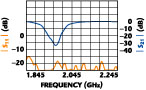
The RX bandpass filter, using the quarter wavelength coupled line technique, is used for the extraction of the RX noise signals.13,14 The characteristics of the implemented RX bandpass filter are shown in Figure 6 . It has a 1.8 dB insertion loss over the RX frequency band and a 24 dB attenuation over the TX frequency band.
|
|
|
|
Fig. 6 Rx bandpass filter characteristics. | |
|
| |
|
Fig. 5 Phase variation as a function of attenuation for the (a) transmit and (b) receive attenuators. |
Fig. 7 Two-tone intermodulation characteristics of the main amplifier before linearization. |

Experimental Results
When the output power of the main amplifier is 36.4 dBm per tone, its two-tone intermodulation distortion is 33.5 dBc, as shown in Figure 7 . The spectrum at the subtracter output is shown in Figure 8 . It indicates that the rejection characteristic of the main carrier signals is 50.7 dBc. The cancellation of the intermodulation distortion signals, shown in Figure 9 , is greater than 31 dB.
|
|
|
|
Fig. 8 Signal spectrum at the output of subtracter. |
Fig. 9 Two-tone intermodulation characteristic of the feedforward amplifier after linearization. |

To show the rejection characteristic of the RX band noise signals effectively, the TX band intermodulation distortion cancellation loop and the RX band noise cancellation loop were individually measured and tuned to have the best signal cancellation over the TX and RX bands by adjusting the variable attenuators and phase shifters. For the measurement of the TX band intermodulation distortion cancellation loop, the RX band noise cancellation loop was disconnected and replaced by a 50 W termination. Also, for the measurement of the RX band noise cancellation loop, the TX band intermodulation distortion cancellation loop was disconnected and replaced by a 50 W termination. Figures 10 and 11 show the TX band intermodulation distortion cancellation loop characteristic and the RX band noise cancellation loop characteristic, respectively. The rejection characteristics of the intermodulation distortion signals and noise signals are more than 24.2 and 21.8 dB over the operating bands. In the RX band noise cancellation loop, there is a group delay variation caused by the RX bandpass filter. This delay variation results in serious limitations of cancellation according to Equation 1. Thus, better rejection for the RX band noise cancellation loop can be expected by decreasing the delay variation characteristics of the RX bandpass filter, which means improvement of the phase balance between the main and RX noise cancellation paths.
|
|
|
|
|
Fig. 10 Transmit-band intermodulation distortion signals cancellation loop characteristics. |
Fig. 11 Receive-band noise signals cancellation loop characteristics. |
Fig. 12 Transmit-band intermodulation distortion signals cancellation and receive-band noise signals cancellation characteristics with and without receive-band noise signals cancellation loop. |

To show the rejection characteristic of the RX band noise signals and the TX band distortion signals effectively, the TX band intermodulation distortion cancellation loop and the RX band noise cancellation loop were connected simultaneously and tuned to have the best signal cancellation over the TX and RX bands by adjusting the variable attenuators and phase shifters. With the RX band noise cancellation loop, the RX band noise signals are reduced by more than 18 dB, which is worse than with the RX band noise cancellation loop alone. Because the cancellation coupler for the RX band noise cancellation loop is connected following the cancellation coupler of the TX band intermodulation distortion cancellation loop, there is some unbalance between noise signals of the RX band noise cancellation loop. Figure 12 shows the TX band intermodulation distortion cancellation and the RX band noise cancellation characteristics with or without the RX band noise cancellation loop. With the TX band intermodulation distortion cancellation and RX band noise cancellation loop, the TX band intermodulation distortion signals can be reduced by more than 26 dB and the RX band noise signals can be reduced by more than 30 dB.
Conclusion
To reduce the RX band noise signals, a new feedforward TX power amplifier with RX band noise cancellation loop is proposed. The power amplifier is implemented for the IMT-2000 basestation frequency band. By employing the RX band noise cancellation loop, the rejection performance of RX band noise signals is improved by more than 30 dB for the full RX band of IMT-2000. Also, the TX intermodulation distortion signals are reduced by more than 26 dB with the feedforward linearization technique. Thus, RX noise signals that are induced into the RX path are decreased and the RX isolation from the transmit duplexer can be relaxed compared with the case of a conventional power amplifier. Therefore, a reduction in cost and occupied volume can be expected by the duplexer with high TX-to-RX isolation characteristic. In addition, the output power of the amplifier can be reduced because of the low TX path insertion loss in the duplexer.
Acknowledgments
The ERA-5SM amplifier is manufactured by Mini-Circuits. The XHL-21336 and MRF-19030 amplifiers are products of Motorola. The KDCNRW30-32-01 coupler is supplied by KMW and the 1A1305-10 coupler by Anaren.
References
1. N. Pothecary, Feedforward Linear Power Amplifiers , Artech House Inc., Norwood, MA, 1999.
2. G. Gonzalez, Microwave Transistor Amplifier Analysis and Design , Prentice Hall, 1997.
3. A.K. Talwar, "Reduction of Noise and Distortion in Amplifiers Using Adaptive Cancellation," IEEE Transactions on Microwave Theory and Techniques , Vol. 42, No. 6, June 1994.
4. D. Myer, "Design Linear Feedforward Amps for PCN Systems," Microwaves & RF , September 1994, pp. 121-133.
5. W. Koprowksi, "A High Power, Low Distortion Feedforward Amplifier," RF Design , July 1994, pp. 48-50.
6. R. Vitkovich and D. Myer, "High Power Feedforward Amplification System," Microwave Journal , Vol. 37, No. 2, February 1994.
7. J. Yamas, "An HF Dynamic Range Amplifier Using Feedforward Techniques," RF Design , July 1994, pp. 50-59.
8. S. Kang, I. Lee and K. Yoo, "Analysis and Design of Feedforward Power Amplifier," IEEE MTT-S International Microwave Symposium Digest , 1997, pp. 1519-1522.
9. M.T. Hickson, D.K. Paul, P. Gardner and K. Konstantinou, "High Efficiency Feedforward Linearizers," Proceedings of the 24th European Microwave Conference , 1994, pp. 819-824.
10. Y.K. Gray Hau, V. Postoyalko and J. R. Richardson, "Design and Characterization of a Microwave Feedforward Amplifier with Improved Wideband Distortion Cancellation," IEEE Transactions on Microwave Theory and Techniques , Vol. 49, No. 1, January 2001.
11. S.K. Koul and B. Bhat, Microwave and Millimeter-wave Phase Shifter , Artech House Inc., Norwood, MA, 1991.
12. Y.C. Jeong, "Design of a Novel Vector Modulator," Microwave Journal , Vol. 44, No. 10, October 2001, pp. 156-162.
13. David M. Pozar, Microwave Engineering , Wiley, 1998, pp. 422-494.
14. I. Bahl and P. Bhartla, Microwave Solid State Circuit Design , Wiley, 1988, pp. 237-293.
Yong-Chae Jeong received his BSEE and MSEE degrees in electronics engineering from Sogang University, Seoul, South Korea, in 1989 and 1991, respectively. From 1989 to 1991 he worked as a senior engineer with Samsung Electronics. In 1996 he received his PhD in electronics engineering from Sogang University. In 1998 he joined the division of electronics and information engineering, and the Institute of Information and Communication at Chonbuk National University, Chonju, South Korea. He is an associate professor and is currently teaching and conducting research in the area of microwave devices and basestation amplifiers.