

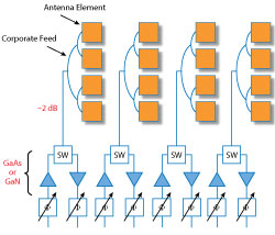
Figure 2 Column-fed array with RF front-end outside the antenna array.
Column-Fed Array
The first active antenna architecture can be called a column- or row-fed array (see Figure 2). In this approach, control ICs are mounted outside the array and drive a single column, with a single gain/phase setting common to all elements in the column. A corporate feed structure is typically employed between the control ICs and the radiating elements. For simplicity, Figure 2 shows just four columns with four elements per column; however, any number of columns and elements per column can be used.
The control ICs may be transmit only, receive only or may support transmit/receive time-division duplexing with a SPDT switch, as indicated in Figure 2. A key advantage to this implementation is mounting the control ICs outside the array area, so the physical size and number of ICs is not critical. This enables high RF power technologies such as GaAs or GaN to drive the column; the result is very high RF power per element, enabling high transmit EIRP from a relatively small array. By simultaneously driving the columns from both top and bottom, the array can be dual polarized. With this approach, the corporate feeds driven from one side of the array energize vertical feeds to the elements, while the corporate feeds from the other side energize the horizontal feeds.
The main advantages of this architecture are
- high RF power per element
- only N control IC RF chains are required per N columns
- the ICs are not constrained to fit within the lattice of the array, since they are outside the array area.
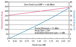
Figure 3 To overcome feed loss, the size of the array must be increased to achieve the required EIRP.
This last advantage is critical to GaAs or GaN solutions, as both semiconductor technologies lack the level of functional integration required to fit all of the control electronics within the typical λ/2 lattice of the array at mmWave.
The first and most obvious challenge for this architecture is that the control ICs are off the array; hence, feed lines must be used to route RF energy to and from the radiating elements. These lines add insertion loss at the worst possible location in any radio, i.e., at the front-end. Adding the ohmic loss of the corporate feed network, the impact on EIRP efficiency and G/T (receive noise figure) efficiency is profound. This increases antenna cost, since the array must be oversized to compensate for the losses. In Figure 2, 2 dB feed loss is shown; however, the actual loss will depend on how the feed lines are implemented. Figure 3 shows the effect of feed loss on transmitter EIRP. As feed loss increases, the array must be oversized to achieve the required EIRP. In this example of a 256-element array with +15 dBm transmit power per element, an imbedded element gain of +5 dBi and a feed loss of 2 dB, the array must be increased to 322 elements (a 26 percent increase) to maintain the targeted +68 dBmi EIRP. EIRP follows 20log(N), where N is the number of elements in the array, so EIRP can be recovered quickly by adding a few more elements.
However, the effect of feed loss is more significant for a receiver (see Figure 4). As feed loss increases, the array must be significantly oversized to achieve the required G/T. In this example of a 1024-element array with a 4 dB receiver noise figure, an imbedded element gain of +5 dBi and a feed loss of 2 dB, the array must be increased to 2019 elements (a 97 percent increase) to maintain the targeted G/T of +8.7 dB/K. The reason feed loss hurts the receiver much more than the transmitter is twofold: receiver G/T follows 10log(N), where N is the number of elements in the array, so it takes more elements to recover front-end loss. Secondly, depending on the values of feed loss and receiver noise figure, the feed loss can affect G/T by more than 1 dB/dB as indicated in Figure 5. For practical values of mmWave receiver noise figure (3 to 5 dB), G/T varies with feed loss by 1.5 to 2 dB/dB, meaning that a 1 dB feed loss degrades G/T by 1.5 to 2 dB. While GaAs- and GaN-based, column-fed, planar arrays offer high EIRP, their receive performance suffers significantly.
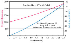
Figure 4 To overcome feed loss, the size of the array must be increased to achieve the required G/T.
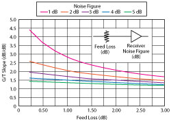
Figure 5 Slope of G/T vs. feed loss and noise figure.
Another challenge with the column-fed architecture is that it only supports one-dimensional beam steering, i.e., azimuth (AZ) scanning only for the example in Figure 2. This lack of two-dimensional (2D) steering is probably acceptable for early, 5G, fixed wireless access applications; however, it is not suitable for applications such as low and medium orbit satellite (LEO/MEO SATCOM), mobile SATCOM and dense urban small cells for 5G, where 2D scan capability will be required.
Another challenge using GaAs or GaN control ICs is their inability to self-compensate for the amplitude and phase variations in the ICs. Lacking the ability to correct for part-to-part variations, which can exceed ±2 dB in |S21| and ±100 degrees in ∠S21, forces array calibration, which adds significant cost to the active antenna system.
There is also a concern that relying on 6-inch GaAs and GaN technologies, only available from a small group of global suppliers, limits how cost-effective these solutions can be in volume production. The ability to achieve low cost is limited by the need for precision lithography for millimeter wave frequencies, such as e-beam gate definition. Finally, using depletion-mode semiconductor technologies such as GaAs or GaN requires dual-supply voltages, positive and negative, which adds system cost. To protect these devices during turn-on and turn-off, DC sequencers are needed to prevent applying a positive voltage without the negative voltage, which increases system complexity and cost.