
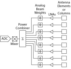
Figure 8 Analog beamforming.
Beamforming
Three general beamforming architectures are used in active antennas: analog, digital and hybrid beamforming. This section describes each approach at a high level, compares their pros and cons and discusses how the column-fed and all-silicon architectures are impacted. While the following block diagrams denote receivers, transmitter block diagrams look similar, just reversed in direction and using digital-to-analog converters (DAC) instead of analog-to-digital converters (ADC).
Analog beamforming (see Figure 8) uses an analog beam weight at each element in the array with the all-silicon architecture or at each column in the array with the column-fed architecture. After the analog beam weights are applied, a coherent power summation forms the beam, followed by a suitable frequency down-converter and ADC to complete the receive antenna system. Table 1 summarizes the advantages and disadvantages.
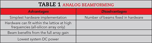
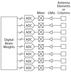
Figure 9 Digital beamforming.
With digital beamforming (see Figure 9), the beams are formed using complex digital weights rather than analog weights. To do this, a full receiver chain from antenna element to digits is required at every element in the array with the all-silicon architecture or at every column in the array with the column-fed architecture. For full 2D scanning in planar arrays, this is only practical at low frequencies, such as S-Band, where the lattices are large, with room to place the required hardware within the array. This approach is not practical for 2D scanning at mmWave frequencies, since inadequate real estate exists with the tight lattices. Since the column-fed architecture is limited to 1D scanning, it can implement digital beamforming because the electronics resides outside the array. Additionally, since a full receiver is only required at every column, rather than at every element, DC power consumption is reduced.
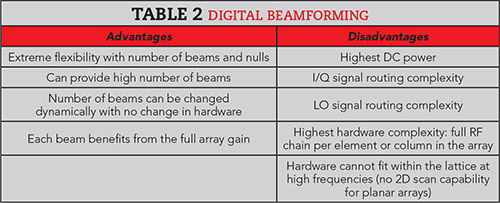
Other significant challenges with digital beamforming include high DC power consumption, especially if large bandwidths are digitized; signal routing complexity, where multiple bits of I and Q data must be routed off the array to the digital processor; and local oscillator (LO) signal routing within the array. On the plus side, if these challenges can be addressed, then this architecture is the most flexible, since multiple beams and nulls can be formed dynamically with no change in hardware, and each beam benefits from the gain of the full array. The advantages and disadvantages are summarized in Table 2.
Hybrid beamforming is a cross between analog and digital beamforming (see Figure 10). An array with hybrid beamforming forms an analog beam from a portion of the full array (sub-array), with the resulting beams as illustrated in Figure 11. The figure shows the wide beam of the imbedded element, the narrower beam formed by the analog sub-array and two digitally-formed beams. For simplicity, only two digital beams are shown, but many beams can be formed within the analog beam. Both the all-silicon and column-fed architectures can use hybrid beamforming. The beauty of hybrid beamforming is it
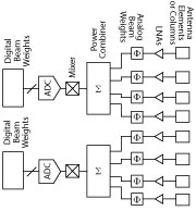
Figure 10 Hybrid beamforming on the receive path.
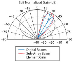
Figure 11 Example beams with hybrid beamforming.
- can be used at mmWave frequencies
- provides the digital flexibility of being able to dynamically form many beams and nulls with no change in hardware
- does not require a full RF chain per element, only a full RF chain per sub-array.
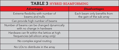
The main downside is that no single beam benefits from the gain of the full array. However, with the many advantages that hybrid beamforming offers, it is no wonder that this is the most popular beamforming approach used in emerging 5G communications systems today. The advantages and disadvantages are summarized in Table 3.
Conclusion
Active mmWave antennas for 5G and satellite communications will reach unprecedented production volumes over the next few years, and two predominant planar architectures have emerged. One is based on GaAs or GaN ICs located off the array and the other uses silicon ICs imbedded within the array. While the GaAs/GaN solution offers very high EIRP capability, the approach has significant limitations, including poor receiver performance from high feed loss and the inability to self-calibrate. The architecture is limited to 1D scanning, requires bias support circuitry such as DC sequencers and offers a challenging path to low production cost.
In contrast, all-silicon active antennas overcome these limitations. While limited in transmit power per element, the architecture offers a clear path to high volume manufacturability and ultra-low production cost, while meeting all key considerations for active mmWave antennas.