
In RF devices, such as power amplifiers and mixers, couplers and combiners/dividers are required for their operation.1 Especially, Wilkinson power dividers and branch-line couplers have been widely used for power splitting/combining.2-6 However, conventional combiners/dividers employ quarter-wavelength lines,2-4 which has been an obstacle to the realization of miniaturized on-chip power splitting/combining circuits. In this work, using a π-type multiple coupled microstrip line structure (MCMLS),7 a miniaturized on-chip power divider was realized on a GaAs substrate. An R-C-R circuit structure, consisting of two resistors and a capacitor, was connected between the two output ports of the power divider to improve its isolation characteristic.
Design of a Multiple Coupled Line Power Divider Employing R-C-R Isolation Compensation Circuit
Figure 1 shows a quarter-wavelength line and a conventional π-type single transmission line structure (STLS)5,6 equivalent to the quarter-wavelength line. Using the π-type STLS, miniaturized couplers were fabricated on semiconducting substrates.5,6 However, as the line length l of the π-type STLS becomes shorter, the characteristic impedance Z of the STLS becomes larger, which makes it difficult to fabricate ultra-compact passive components, using the π-type STLS.5,6 For example, if the line length of the π-type STLS on a GaAs substrate becomes less than λ/12, the characteristic impedance Z becomes higher than 100 Ω. A transmission line whose characteristic impedance is higher than 100 Ω cannot be easily realized on semiconducting substrates, due to a loss originating from its very thin line width.5,6
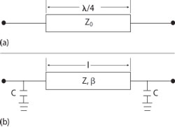
Fig. 1 A quarter-wavelength microstrip line (a) and a conventional π-type single transmission line structure (STLS) (b).
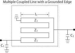
Figure 2 π-type multiple coupled microstrip line structure (MCMLS).
In order to overcome the above problem for the conventional π-type transmission line, a π-type MCMLS was employed. Figure 2 shows the π-type MCMLS.7 According to a previous study,7 the characteristic impedance Z1 of each line comprising the multiple coupled microstrip line was highly reduced by grounding the edge. Therefore, the single line of π-type circuit was replaced by the multiple coupled lines with a grounded edge, which facilitated the realization of miniaturized on-chip passive components on a semiconducting substrate.
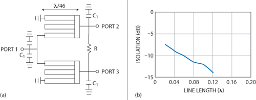
Figure 3 Multiple coupled line power divider using one resistor (a) and isolation characteristics as a function of line length (b).
First, a multiple coupled line power divider was fabricated, employing only one resistor on a GaAs substrate. Figure 3 shows the power divider and its isolation characteristic. As shown, like for a conventional Wilkinson power divider, only one resistor was connected between the two output ports. The line length was reduced to λ/46 by using the π-type MCMLS. Unlike the π-type STLS, even though the line length is highly reduced, the characteristic impedance was not rapidly increased. The characteristic impedance of the π-type STLS, with a line length of λ/46, is 200 Ω, which cannot be realized on a semiconductor substrate. In the case of the π-type MCMLS, however, if the line length is λ/46, the characteristic impedance Z1 becomes 60 Ω, which can be easily realized on a semiconductor substrate. The power divider shows an isolation worse than −10 dB in a range of line length shorter than 0.06 λ, which is unsatisfactory for application to a power divider. Especially, a shorter line length results in worse isolation. According to an investigation of the basic characteristics of multiple coupled lines, the isolation characteristic of RF components employing multiple coupled lines is highly deteriorated, due to the parasitic elements between the lines.7,8 In a previous study,7 using the π-type MCMLS, a power divider without an R-C-R compensation circuit was fabricated on PCB. Even though it was fabricated on PCB, the degradation of the isolation characteristic was also observed.7
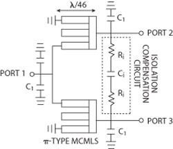
Fig. 4 Proposed multiple coupled lines power divider using an R-C-R isolation compensation circuit.
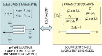
Figure 5 π-type multiple coupled microstrip line structure (MCMLS) and its equivalent microstrip line model with a characteristic impedance Zi and propagation constant ßi.
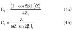
In this work, an R-C-R circuit structure was employed to improve the isolation characteristic of the power divider. Figure 4 shows the proposed power divider. As shown in this figure, the R-C-R circuit structure, consisting of two resistors and a capacitor, was connected between the two output ports. The isolation compensation theory and design procedure can be explained as follows. First, as shown in Figure 5, a single microstrip line model equivalent to the π-type MCMLS was extracted. The equivalent characteristic impedance Zi and propagation constant βi of the single microstrip line model were extracted so that the measured Z parameter of π-type MCMLS coincides with the two-port Z parameter equation of the single microstrip line model. Using the above method, the Zi and βi can be given by
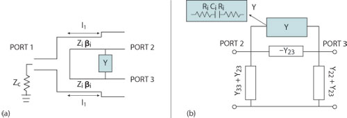
Figure 6 Wilkinson power divider with port 1 terminated and ports 2 and 3 excited (a) and its equivalent circuit (b).
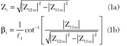
where Z12m and Z11m are the measured Z parameters of the π-type MCMLS, and l1 is the length of the π-type MCMLS. Using theZi and βi, the value of Ri and Ci of the R-C-R circuit were chosen so that the isolation of the proposed power divider was infinite. Figure 6 shows the proposed power divider with port 1 terminated and ports 2 and 3 excited. The π-type MCMLS was expressed as an equivalent microstrip line model with Zi and βi. Generally, a Wilkinson power divider with port 1 terminated can be expressed as a simple equivalent circuit shown.2 Y22, Y23 and Y33 are Y parameters of the three-port equivalent circuit. According to equivalent circuit analysis of the Wilkinson power divider,2 Y23 can be expressed as follows
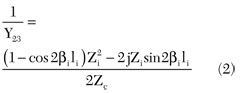
In the equivalent circuit, the R-C-R circuit and −Y23 are connected with each other in parallel. Therefore, it is clear that ports 2 and 3 will be uncoupled if Y =Y23, so that the total admittance between ports 2 and 3 vanished. In the conventional Wilkinson power divider, the line length is λ/4 and βl is π/2. Therefore, from Equation 2, it is clear that Y23 becomes a real number, and only a resistor is connected between two isolation ports. In the proposed power divider, however, the line length is λ/46 and Y23 becomes a complex number. Therefore, if an R-C-R circuit is used, the admittance of the R-C-R circuit becomes a complex number and Y =Y23 can be satisfied as follows
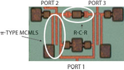
Figure 7 Photograph of the multiple coupled line power divider.
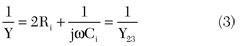
From the above equation, the following results can be obtained
In this work, Ri and Ci are 3.04 Ω and 2.7 pF, respectively.
Measured Results
Figure 7 shows a photograph of the proposed Wilkinson power divider, which was fabricated on a GaAs substrate. The line length is 260 μm and the shunt capacitor C1 is 1.83 pF. The size of the proposed Wilkinson power divider is 0.304 mm2, which is 12.1 percent of a conventional Wilkinson power divider employing quarter-wave lines. The sizes of the proposed Wilkinson power divider and conventional ones on a GaAs substrate are summarized in Table 1.
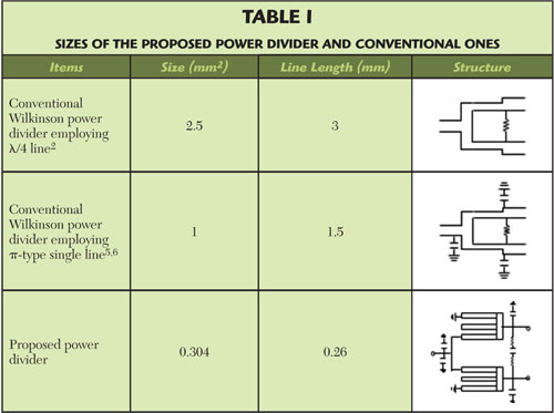
Figure 8 shows the measured power division, isolation characteristics and phase division characteristics for the proposed power divider. As shown, equal power division characteristics for all frequencies can be observed. S21 and S31 exhibit a value of −5.4 dB at a center frequency of 8 GHz. In the frequency range of 4.5 to 8.8 GHz, S21 and S31 show a value of −4.9 ±1 dB, which is comparable to a conventional on-chip Wilkinson power divider.5,6 Equal phase division characteristics can also be seen for all frequencies, because a perfect symmetry was maintained in the shape of the proposed power divider. The isolation, (S23) shows a value of −23.5 dB at 8 GHz and values better than −11 dB for all frequencies. To confirm the effectiveness of the R-C-R isolation compensation circuit, the isolation characteristic of the proposed power divider was compared with that of the power divider employing only a resistor. Figure 9 shows the measured isolation characteristics of the power dividers. The isolation was measured at 8 GHz. As shown, the isolation characteristic of the proposed power divider was highly improved by using the R-C-R isolation compensation circuit. If a transmission line with a length of 0.0217λ (=λ/46) is used, the proposed power divider employing an R-C-R circuit shows an isolation of −23.5 dB, while the power divider employing only resistor shows an isolation of −7.5 dB.
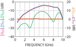
Fig. 8 Measured RF characteristics of the proposed power divider using an R-C-R isolation compensation circuit.
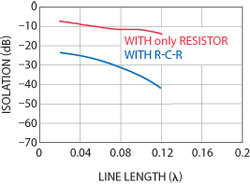
Figure 9 Measured isolation of the proposed power divided at 8 GHz with only a resistor and with an R-C-R circuit.
Conclusion
In this work, using an MCMLS and an R-C-R isolation compensation circuit, an ultra-compact and high isolation power divider was fabricated on a GaAs substrate. The line length of the power divider was reduced to λ/46 by using the π-type MCMLS. The size of the proposed power divider was 0.304 mm2, which was 12.1 percent of a conventional Wilkinson power divider on a GaAs substrate. An R-C-R isolation compensation circuit was employed to highly improve the isolation characteristic of the power divider. If a transmission line with a length of 0.0217λ (=λ/46) is used, the proposed power divider, employing an R-C-R circuit, showed an isolation of −23.5 dB, while the power divider employing only resistor showed an isolation of −7.5 dB. The proposed power divider showed good RF performances in the C-/X-Band. The isolation was better than −11 dB in the C-/X-Band. Owing to the perfect symmetry in its shape, the proposed power divider showed equal power and equal phase division characteristics for all frequencies. The power division characteristic in the C-/X-Band, S21 and S31, showed a value of −4.9 ±1 dB, which was comparable to a conventional on-chip Wilkinson power divider. The above results indicate that the proposed power divider is a promising candidate for application to power coupling and dividing of RF devices on MMIC.
Acknowledgments
This work was supported by a Grant of the Korean Ministry of Education, Science and Technology (The Regional Core Research Program/Institute of Logistics Information Technology). This research was also supported by the Basic Science Research Program through the National Research Foundation of Korea (NRF) funded by the Ministry of Education, Science and Technology (2010-0007452). This work was also financially supported by the Ministry of Knowledge Economy (MKE) and the Korea Industrial Technology Foundation (KOTEF) through the Human Resource Training Project for Strategic Technology.
References
- D.R. Webster, G. Ataei and D.G. Haigh, “Low-Distortion MMIC Power Amplifier Using a New Form of Derivative Superposition,” IEEE Transactions on Microwave Theory and Techniques, Vol. 49, No. 2, February 2001, pp. 328-332.
- R.E. Collin, Foundation of Microwave Engineering, 2nd edition, McGraw-Hill, New York, NY, 1992.
- J.C. Chiu, J.M. Lin and Y.H. Weang, “A Novel Planar Three-Way Power Divider,” IEEE Microwaves and Wireless Components Letters, Vol. 16, No. 8, August 2006, pp. 449-451.
- X. Li, Y.J. Yang, L. Yang, S.X. Gong, T. Hong, X. Chen and Y.J. Zhang, “Novel Design of Unequal Wilkinson Power Divider or Dual-Band Operation,” Microwave and Optical Technology Letters, Vol. 52, No. 8, August 2010, pp. 1736-1739.
- T. Hirota, A. Minakawa and M. Muraguchi, “Reduced-Size Branch-Line and Rat-Race Hybrids for Uniplanar MMICs,” IEEE Transactions on Microwave Theory and Techniques, Vol. 38, No. 3, March 1991, pp. 270-275.
- M.C. Scardelletti, G.E. Ponchak and T.M. Weller, “Miniaturized Wilkinson Power Dividers UtiliZing Capacitive Loading,” IEEE Microwaves and Wireless Components Letters, Vol. 12, No. 1, January 2002, pp. 6-8.
- Y.B. Park, H.N. Joh, S.H. Kim, Y. Yun and I.H. Kang, “Highly Miniaturized Passive Components Employing Novel π-type Multiple Coupled Microstrip Lines,” Proceeding of the 10th Conference On Science and Technology, 2007, pp.135-138.
- B.C. Wadell, Transmission Line Design Handbook, Artech House, Norwood, MA, 1991.
Young Yun received his B.S. degree in electronic engineering from Yonsei University, Seoul, Korea, in 1993, his M.S. degree in electrical and electronic engineering from Pohang University of Science and Technology, Pohang, Korea, in 1995, and his Ph.D. degree in electrical engineering from Osaka University, Osaka, Japan, in 1999. From 1999 to 2003, he worked as an engineer in Matsushita Electric Industrial Company Ltd. (Panasonic), Osaka, Japan, where he was engaged in the research and development of monolithic microwave ICs (MMIC) for wireless communications. In 2003, he joined the Dept. of Radio Sciences and Engineering, Korea Maritime University, Busan, Korea. His research interests include design and measurement for RF/microwave and millimeter-wave IC and design and fabrication for HEMT and HBT.