
In broadband communication systems, such as ultra-wideband (UWB), low impedance transformation is required for impedance matching between active devices because the input and output impedances of the FETs are much lower than 50 Ω in the RF band.1 Therefore, for efficient impedance matching in a radio frequency integrated circuit (RFIC) in a broadband communication system, a broadband and low impedance transformer performing low impedance transformation between active and passive devices is indispensable and should be highly miniaturized for integration in RFICs.
λ/4 impedance transformers have been widely used for comparatively broad bandwidth.2 However, conventional impedance transformers have been fabricated outside of RFICs, due to their large size, and used for applications to high impedance transformation (in the range of 40 to 70 Ω) because the line width of the coplanar waveguide with a low impedance is very large and cannot be realized on a RFIC. For example, the line width W should be 1000 μm to obtain a characteristic impedance Z0 of 20 Ω from the conventional coplanar waveguide on silicon substrate with a height of 600 μm.
In this work, in order to realize a highly miniaturized and low impedance on-chip transformer, a multi-section transformer was fabricated using a periodically arrayed grounded-strip structure (PAGS) on silicon substrate. For ultra broadband operation, it was designed using the Chebyshev polynomials design technique.

Figure 1 The structure of a coplanar waveguide using a PAGS.
A Coplanar Waveguide Using A PAGS on Silicon Substrate
A coplanar waveguide, employing a slow wave structure, was fabricated on a GaAs substrate for the first time.6 A miniaturized passive component was recently proposed, employing a slow-wave structure on silicon substrate.3 Figure 1 shows the structure of the coplanar waveguide employing a PAGS. As shown, the PAGS is placed at the interface between the SiO2 film and the silicon substrate, and is electrically connected to the top-side ground planes (GND planes) through the contacts. Therefore, the PAGS is grounded through the GND planes.

As is well known, a conventional coplanar waveguide without a PAGS has only a periodical capacitance Ca per unit length, while the coplanar waveguide employing a PAGS has an additional capacitance Cb, as well as Ca, due to the PAGS. Cb is the capacitance between the line and PAGS. In other words, the total capacitance (per unit length) of the coplanar waveguide employing a PAGS corresponds to Ca + Cb, but it only corresponds to Ca for a conventional coplanar waveguide without a PAGS. Therefore, the coplanar waveguide employing a PAGS exhibits a much shorter guided-wavelength (λg) and a lower characteristic impedance (Z0) than a conventional one, because λg and Z0 are inversely proportional to the periodical capacitance; in other words, λg = 1/ƒ¦(LC)0.5] and Z0 = (L/C)0.5. As shown in Table 1, at 40 GHz the wavelength of a conventional coplanar waveguide on silicon substrate is 2.95 mm, while it is 1.86 mm for a coplanar waveguide employing a PAGS.

In this structure, the value for Z0 can be easily controlled by only changing the spacing T, because an increase in T results in a reduction of Z0, due to an increase in Cb. Actually, as shown in Table 2, low impedance values of Z0 were obtained from 30 to 70 Ω by only changing T. In this work, the distance L between the unit strip and the height of silicon substrate are 20 and 600 μm, respectively. In the Table, T = 0 corresponds to a conventional coplanar waveguide without a PAGS.

Figure 2 Schematic circuit of a multi-section λ/4 impedance transformer using a PAGS.
A Highly Miniaturized Multi-section Transformer Employing PAGS on Substrate
Using the coplanar waveguide employing a PAGS, a highly miniaturized and low impedance on-chip transformer employing multi-section lines was developed for broadband applications. For broadband operation, a multi-section transformer was designed using the Chebyshev function. Figure 2 shows a multi-section transformer. For broad bandwidth, the reflection coefficient should follow a Chebyshev function response, and the following equations should be satisfied:2

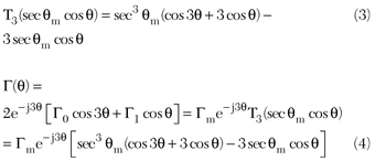
where Γm and TN are a maximum value of the reflection coefficient and the nth order Chebyshev polynomial, respectively. N and Γn are the number of sections and the reflection coefficients of the multi-stage transformer. If N, Γm, ZL and Z0 are determined, secθm can be obtained from Equation 2. In this work, a three-section transformer was designed to match a 50 Ω load to a 19 Ω line, with Γm = 0.05. From Equations 3 and 1b, with N = 3, Equation 4 can be obtained.
From the above equation, the following results can be obtained:

Then the characteristic impedances of the three-section transformer are


Figure 3 Photograph of the on-chip multi-section impedance transformer using PAGS on silicon substrate.
The characteristic impedances Z1 = 26 Ω, Z2 = 35 Ω and Z3 = 43 Ω from N = 3, ZL = 50 Ω and Z0 = 19 Ω are obtained. A photograph of the three-section transformer is shown in Figure 3. The length of each section of the λ/4 transformer, L1, L2 and L3 are 0.38, 0.44 and 0.485 mm, respectively. Therefore, the size of the transformer including via holes is 0.261 mm2, which is 8.7 percent of the size of the transformer fabricated from a conventional coplanar waveguide. This result is summarized in Table 3.

The measured return loss S11 and the insertion loss S21 of the three-section transformer are shown in Figure 4, respectively. The measured S11 of the single section transformer was also plotted for comparison. Compared with the single section transformer, the three-section transformer shows a much broader bandwidth with ripples. The three-section transformer exhibits return loss values better than 10 dB from 8 to 49.5 GHz, and the insertion loss values are 1.5 ± 1 dB in the same frequency range, which is 1.15 ± 0.76 dB/mm for a length of 1 mm (the length of the multi-section transformer is 1.305 mm). Considering that a silicon substrate is lossy due to its high conductivity,5-9 the above insertion loss is comparatively small, and is sufficiently low for application to silicon RFICs. These results indicate that the highly miniaturized multi-section impedance transformer is a promising candidate for application to low impedance transformation in ultra broadband applications.

Figure 4 Measured return loss and insertion loss of the three-section transformer.
Conclusion
Using a coplanar waveguide employing a PAGS on silicon substrate, a highly miniaturized on-chip transformer was developed for application in ultra broadband, low impedance transformation. For ultra broadband operation, the multi-section transformer was designed using the Chebyshev polynomials design technique. The impedances of a three-section transformer were determined so that the reflection coefficient of the transformer would be a Chebyshev function response. The three-section transformer exhibited return loss values better than 10 dB from 8 to 49.5 GHz; the insertion loss values are 1.15 ± 0.76 dB/mm in the above frequency range. Its size is 0.026 m2 on a silicon substrate, which is 8.7 percent of the one fabricated with a conventional coplanar waveguide on silicon substrate. These results reveal that the highly miniaturized multi-section impedance transformer is a promising candidate for application to low impedance transformation in ultra broadband.
Acknowledgment
This work was sponsored by the ETRI System Semiconductor Industry Promotion Center, Human Resource Development Project for SoC Convergence.
References
- Y. Yun, T. Fukuda, T. Kunihisa and O. Ishikawa, “A High Performance Downconverter MMIC for DBS Applications,” IEICE Transactions on Electronics, Vol. E84-C, No. 11, November 2001, pp. 1679-1688.
- D.M. Pozar, Microwave Engineering, Addison-Wesley, Reading, MA, 1990.
- Y. Yun, Y.B. Park, S.K. Kang, I.H. Kang, J.W. Jung and K.H. Park, “Miniaturized On-chip Branch-line Coupler Employing Periodically Arrayed Grounded-strip Structure for Application to Silicon RFIC,” Microwave Journal, Vol. 52, No. 12, December 2009, pp. 82-90.
- R.E. Collin, Foundations for Microwave Engineering, McGraw-Hill, New York, NY, 1966.
- M. Zargari and D. Su, “Challenges in Designing CMOS Wireless Systems-on-a-Chip,” IEICE Transactions on Electronics, Vol. E90-C, No. 6, June 2007, pp. 1142-1148.
- H. Hasegawa, “Cross-tie Slow-wave Coplanar Waveguide on Semi-insulating GaAs Substrate,” Electronics Letters, Vol. 17, No. 25, December 1981, pp. 940-941.
- J.R. Long, “Passive Components for Silicon RF and MMIC Design,” IEICE Transactions on Electronics, Vol. E86-C, No. 6, June 2003, pp. 1022-1031.
- K. Masu, K. Okada and H. Ito, “RF Passive Components Using Metal Line on Si CMOS,” IEICE Transactions on Electronics, Vol. E89-C, No. 6, June 2006, pp. 681-691.
- R. Lowther and S.G. Lee, “On-chip Interconnect Lines with Patterned Ground Shields,” IEEE Microwave and Guided Wave Letters, Vol. 10, No. 2, February 2000, pp. 49-51.
Young Yun received his BS degree in electronic engineering from Yonsei University, Seoul, Korea, in 1993, his MS degree in electrical and electronic engineering from Pohang University of Science and Technology (POSTECH), Pohang, Korea, in 1995, and his PhD degree in electrical engineering from Osaka University, Osaka, Japan, in 1999. From 1999 to 2003, he worked as an engineer for Matsushita Electric Industrial Co. Ltd. (Panasonic), Osaka, Japan, where he was engaged in the research and development of monolithic microwave ICs (MMIC) for wireless communications. In 2003, he joined the department of radio sciences and engineering, Korea Maritime University, Busan, Korea. He is currently an associate professor whose research interests include the design and measurement for RF/microwave and millimeter-wave IC, and the design and fabrication for HEMT and HBT.