

In this article, we take measurements of capacitor impedance curves and examine the results. It seems simple, but it reveals several interesting behaviors.
Let’s start this part with a quiz:
Q: How many different capacitor devices can you identify in the capacitor impedance plots below?
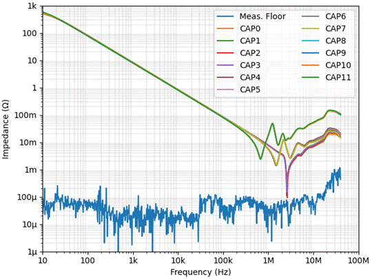
Fig. 14–1. Quiz to identify capacitors
Throughout this article, you will find the answer step-by-step.
A Quick History
To get a better understanding of the material, there are many great articles from PI (Power Integrity) pioneers published around 2005. See references below: [1] [2] [3] [4] [5]
I thank Dr. István Novák (Samtec) for answering my questions and helping me understand his papers.
My Motivation
Around 15 years ago, during bench testing—and before I fully understood the DesignCon discussions mentioned above—I noticed that parallel placement of multiple MLCC devices with the same part number lowers the self-resonant quality factor Q.
Here, I put a spotlight on this behavior in a modern manner applicable to today’s PI engineering community.
Measurement Method
To measure the capacitor impedance curves, I use our PI golden standard:
2-Port Shunt-Through
Note that all tests are performed at zero DC bias.
Target MLCC Device (Part Number)
I picked an MLCC device Würth Elektronik 885 012 14 003.
- Capacitance: 4.7 μF
- Voltage rating: 100 V
- Grade: X7R
- Size: 5.7 mm × 5.0 mm × 2.5 mm
The main reason for choosing this particular MLCC is its size. When I measure parallel placement of these MLCC units, a pair forms a 5.0 mm × 5.0 mm block eliminating X-Y-Z dimensional differences.
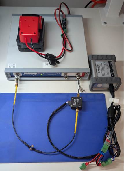
- Omicron-Lab Bode 100, Vector Network Analyzer, powered by an 18 V hand-tool Li-ion battery pack.
- Picotest J2114A-MOD, Modified Prototype High CMRR Isolation Amplifier, powered by a Picotest. J2171A, High PSRR Regulated Adapter; courtesy of my mentor Steve Sandler at Picotest for access to this prototype product.
- Zebax ZX00SMAS-J/-P, SMA connector to 2 pin Socket cable assembly.
Fig. 14–2. Measurement Setup (Note: Photographed after testing, on a clean background for clarity. Device and results unchanged.) |
- A pair of long (jack at both ends) 2 × 1 pin-headers, mating the Zebax sockets for both force and sense.
- A pair of H-shaped folded copper sheets, soldered the pin-headers at the center bar,
it’s a combination of two folded copper sheets, ⊓ -shaped and ⊔ -shaped forming the H. - A controlled gap is maintained between these two H-shaped copper mounting pieces.
- Target capacitor devices are solder-mounted across the pair of H-shaped copper pieces.
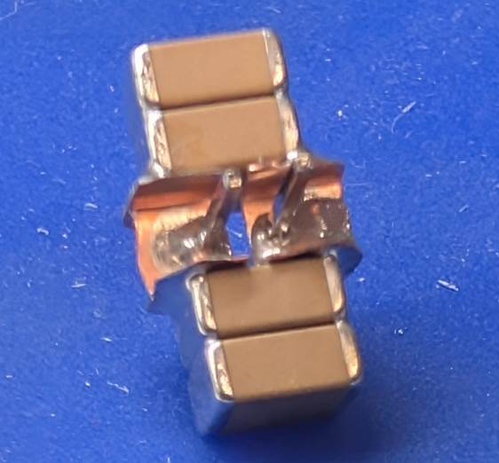
Fig. 14–3. DUT #Case-1 on H-shaped Adapter
The advantage of this jig is that both force and sense ports probe the same point through the copper sheet thickness, and the T-shaped portion (half of the H) touches the center-bottom of the capacitor devices. This gives us a clear definition of the *Z-direction* in our measurement sensitivity for 3-D orientations.
Calibration and Known References
As usual, we strictly follow PI Measurement 101:
Calibrate the setup first, then start measurements from known targets
We run a Short/Open/Load (SOL) calibration of the Bode 100 unit.
As Steve Sandler pointed out in [6], I paid special attention to the "short" calibration step.
After a successful SOL calibration, I checked the "short," from the calibration process as my measurement floor / limit. Then, I measured a couple of known devices. Below are approximate SMU (Source-Measure Unit) DC resistance readings that are good enough for this writing project.
Cal. Short | Short of the SOL Calibration, SMU reading of DC resistance ~40 μΩ, referred as Measurement Floor |
Short "H" | Short on the H-shaped adapter, SMU reading of DC resistance ~150 μΩ |
4-parallel 3.85 nH | Chip Inductors, Face-value target of 0.963 nH (= 3.85 nH / 4), Actual curve cursor reading of 0.932 nH, in its inductance, Actual curve cursor reading of 0.622 μΩ, in its resistance, SMU reading of DC resistance ~750 μΩ |
4-parallel 1 mΩ | Current Sense Resistors, Face-value target of 250 μΩ, Actual curve cursor reading of 0.352 μΩ, SMU reading of DC resistance ~390 μΩ, |

Fig. 14–4. Known Reference Devices
Some notes:
- The J2114A-MOD is outside its operational bandwidth beyond 10 MHz.
- From its magnetic-flux-cancellation structure, the 4-parallel 1 mΩ network must be lower in parasitic inductance, which is confirmed by the curves below.
- By probing the curve, the Short H has 5.16 mΩ at 10 MHz. This corresponds to approximately 82.2 pH parasitic inductance.
- Compared with the 4-parallel 3.85 nH network, we see a clean +20 dB/dec characteristic, confirming that the Short H behaves as an inductor at higher frequencies.
Capacitance Measurement #Case-1
We use the DUT in Fig. 14-3 for our first capacitor impedance measurement.
This setup is:
- 2-parallel placements on both sides of the H-shaped, with
- Z-direction 2 stacking MLCCs
While stacking MLCC devices may seem odd, it is intentional and supports the main message, which I’ll explain later.
Unlike SMA connector-base fixtures commonly chosen by many PI experts, this 2 × 1 pin-header adapter has strong advantages:
- We can swap force and sense lines.
- We can swap positive and negative electrodes.
With these two swaps, we made four curve measurements as shown below.
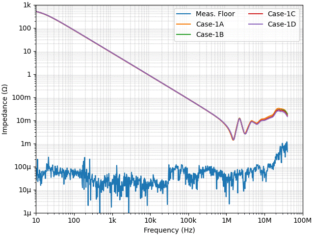
- All four curves overlap very well.
- This confirms an MLCC is non-polar (non-polarized).
- The H-shaped adapter is symmetric.
- This 2-port shunt-through measurement is repeatable.
- We can clearly see multiple resonances and anti-resonances, as a result of standing waves,
as well explained in reference 1. - Because the H-shaped adapter is hand-made, the header pins are not placed at the exact center of the center-bar.
This is observed as two groups of small differences around the 10 MHz region.
Deeper Considerations #Case-1
Based on the papers by Dr. Novák, at the self-resonant frequency (~1.5 MHz, in #Case-1), an MLCC drives current density toward the far end of the electrode stack. Consider this behavior before moving to next measurements.
At the self-resonant point, the MLCC impedance goes down to its minimum equal to ESR (Equivalent Series Resistance).
In a 2-port shunt-through setup, its 50 Ω force line acts as a current source, and we sense a very small voltage response at the 50 Ω sense line.
Put differently: Large current in; small voltage out.
An MLCC device has no DC conduction path; all AC current traverses the dielectric. To conduct large current, a large voltage must exist across the dielectric body. Yet, we observe a small voltage at the measurement ports. The missing factor is the device’s finite height in the Z-direction.
As shown in the picture below (Fig. 14–6), at the mounting surface (Z=0), we see large current in and small voltage out. At the top of the multi-layer stack (Z=Hmax) across the electrodes, we have a larger voltage swing to conduct the large current though the dielectric. In a simple picture, the large input current climbs to the top layer along the electrode plates.
Practically, as Dr. Novák describes, we observe 1/4 standing wave at the main self-resonant frequency (~1.5 MHz). The 1/2 standing wave gives the first anti-resonant maximum (~2.2 MHz for #Case-1), and the 3/4 standing wave gives the second minimum (~3.1 MHz), and so on.
For clarity in this article, the large-size 100 V rating MLCC was chosen illustrate the standing wave effect.
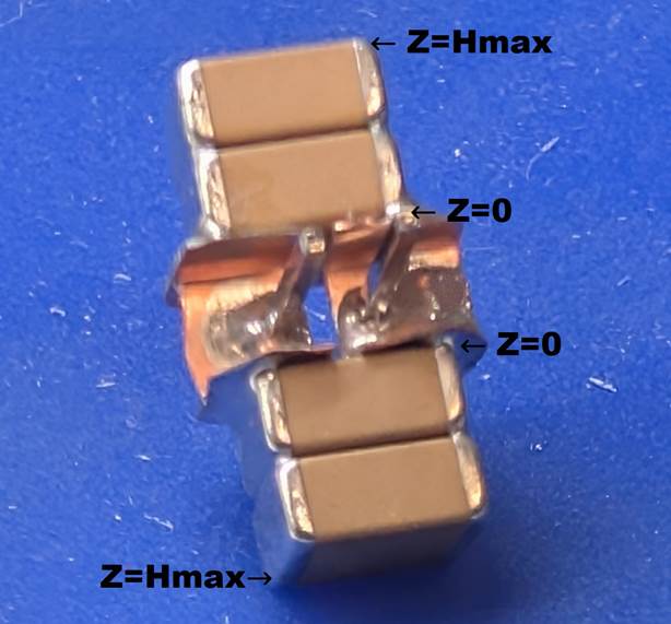
Fig. 14–6. Case-1 DUT Z-direction Travel Length
Capacitance Measurement #Case-2
To follow Dr. Novák’s path, we test a DUT consisting of Z-direction 4 stacking MLCCs.
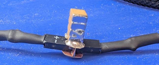
Fig. 14–7. DUT #Case-2 on H-shaped Adapter
We again take four measurements by swapping the 2 × 1 header sockets.
In the plot, guidelines and the previous Case-1A measurement are shown as dotted lines.
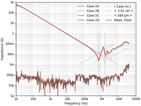
Fig. 14–8. Case-2 Capacitance Curves
- All four curves overlap very well, as in #Case-1.
- We again see multiple resonances and anti-resonances, due to standing waves.
- Because of the longer standing wave travel length, the resonant and anti-resonant frequencies are lower than in #Case-1.
- A –20 dB/dec guideline aligned to the low frequency region of the capacitance yields an estimated 18.7 μF total for this 4-parallel capacitor block..
- From vertical guidelines pointing to the resonant minima:
#Case-1: 1.49 MHz
#Case-2: 680 kHz - Placing +20 dB/dec guidelines that cross the 18.7 μF line at the resonant frequencies, the estimated equivalent series inductance (ESL) values are:
#Case-1: 589 pH
#Case-2: 3.01 nH
Deeper Considerations #Case-2
Per Dr. Novák, in #Case-2, the resonant current tries to climb to the very top layer overall, even if this may seem counterintuitive.
My interpretation: At self-resonance, we must utilize the entire MLCC volume to minimize impedance. To do so, current must be sent to the top layers to use the full dielectric volume. An MLCC can be modeled as an open-ended lossy transmission line exhibiting full reflection at the top layer. [3]
In simple terms, we might expect the ESL of the main resonances to be in a 1:4 ratio as a result of 2× difference in height and 2× difference in parallel blocks. The measured ratio is roughly 1:5 = 3.01-nH:0.589-nH.
As shown in below (Fig. 14–9), a realistic MLCC structure has top and bottom ceramic buffer regions of thickness b that sandwich the main capacitor region of thickness h. A single MLCC top-layer distance from the PCB surface is (h+b). For a 2-stack, the top-layer distance becomes (b+h+b) + (h+b) = (2h+3b).
With a rough assumption of (h = 2b), the height ratio becomes 3:7 = 1:2.33. This structural consideration adjusts the expected ESL ratio to ≈1:4.7, aligning better with the #Case-2 results.
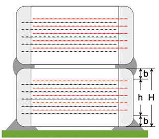
Fig. 14–9. Simplified MLCC Physical Structure
Capacitance Measurement #Case-3
This last measurement yields a very interesting result.
#Case-3 uses a parallel MLCC configuration where each MLCC is standing, rotated 90° from #Case-1 or #Case-2. This is why, throughout this article, we use a pair of 5.0 mm × 2.5 mm devices to form a 5.0 mm × 5.0 mm block. Dimension-wise, #Case-1 and #Case-3 are identical; only the layer orientation is changed.
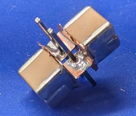
Fig. 14–10. DUT #Case-3 on H-shaped Adapter
Again, we take four measurements by swapping the 2 × 1 header sockets.
The plot includes guidelines from Case-1A and Case-2A as dotted lines.
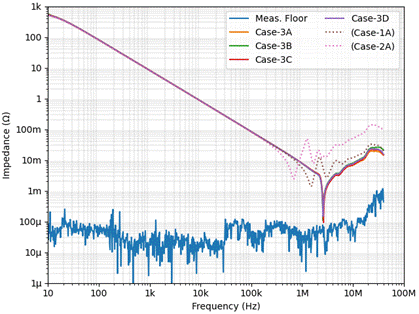
Fig. 14–11. Case-3 Capacitance Curves
- All four curves overlap very well, as in #Case-1 and #Case-2.
- We barely see resonance peaks other than the main strong Q peak at 2.64 MHz.
- The impedance curves look totally different from those in #Case-1 and #Case-2.
- Even though the physical dimensions are identical; only the MLCC layer orientation changes.
Deeper Considerations #Case-3
The main difference between #Case-1 and #Case-3 is whether there is a definitive layer structure in the mounting Z-direction.
In #Case-1, repeating layers in the Z-direction form an open-ended lossy transmission line. [3]
In contrast, #Case-3 has many planes facing the H-shaped adapter at right angles. For a given plane pair, current distribution is two-dimensional in a distributed-parameter conduction plane pair, and clear standing waves do not form in #Case-3.
(See Appendix below.)
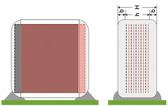
Fig. 14–12. Simplified MLCC Physical Structure in #Case-3
Actual MLCC Tape & Reel
You might think this is merely about manually soldering MLCC devices in unusual orientations or manually stacking them.
Below is a photo of my cut-tape MLCC with a pair of square electrodes from a major supplier. You can see random shadowing on the electrode surface. YES, in tape pockets, it is random whether MLCCs are lying flat or standing.
I checked several cut-tape MLCCs from multiple major suppliers: the orientation in the pockets is random.
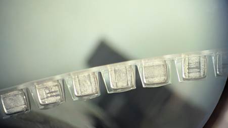
Fig. 14–13. Square-shape Electrode MLCC in Tape & Reel
For some engineers, including those from RF and signal-chain domains, it can be a concerning finding.
The #Case-1, #Case-2 and #Case-3 curves shown here are my take-7 data-set. Before take-7, I encountered six different pitfalls, all caused by this random orientation challenge.
Answer to the Opening Quiz
Answer #1: Only one MLCC part number in Fig. 14-1.
Answer #2: All the same capacitors in parallel but with different placement / mounting / soldering.
Summary
- MLCCs are electrically non-polar, but their impedance is sensitive to the orientation of the multi-layer stack on the PCB.
- When the multi-layer stack is parallel to the PCB surface (Z-direction repeating structure), the impedance shows resonant and anti-resonant peaks due to standing waves in the vertical stack.
- With square electrodes (W = H), devices in tape-and-reel are often randomly oriented with respect to the layer direction; if orientation sensitivity matters, consider non-square devices (W ≠ H).
- Orienting the multi-layer stack perpendicular to the PCB surface yields far fewer secondary peaks, although achieving this orientation reliably in mass production is challenging.
Test conditions in this study: 2-port shunt-through, SOL calibration, 0 V DC bias; device: 4.7 µF / 100 V X7R, 4 parallel.
References
1. István Novák, "A Black-Box Frequency Dependent Model of Capacitors for Frequency Domain Simulations," Proceedings of DesignCon East 2005, September 19 – 21, 2005, Worcester, MA
2. István Novák, "Slow-Wave Causal Model for Multi Layer Ceramic Capacitors," Proceedings of DesignCon 2006, February 6 – 9, 2006, Santa Clara, CA.
3. L. D. Smith, D. Hockanson and K. Kothari, "A transmission-line model for ceramic capacitors for CAD tools based on measured parameters," 52nd Electronic Components and Technology Conference 2002. (Cat. No.02CH37345), San Diego, CA, USA, 2002, pp. 331-336, doi: 10.1109/ECTC.2002.1008116.
4. Larry Smith, "MLC Capacitor Parameters for Accurate Simulation Model," in TF7 “Inductance of Bypass Capacitors; How to Define, How to Measure, How to Simulate” Proceedings of DesignCon 2005, January 31 – February 3, 2005, Santa Clara, CA.
5. M. Shimizu, S. Kazama, T. Hiraoka, “Measurement ESL/ESR of the Passive Components and Compensation of the Fixtures," in TF7 “Inductance of Bypass Capacitors; How to Define, How to Measure, How to Simulate” Proceedings of DesignCon 2005, January 31 – February 3, 2005, Santa Clara, CA.
6. Steve Sandler, "Calibration with De-Embedding for Precise Component Measurements," Signal Integrity Journal, April 19, 2025
Appendix
NOTE: This appendix is for illustration only; parameters and solver details were simplified for clarity. This is qualitative and not scaled to the physical MLCC device we tested above.
Using the ChatGPT5-assisted modeling, we qualitatively visualized the in-plane voltage distribution for the left drawing of Fig 14-12 (#Case-3). See the prompt input lines, listed at the end of this session.
We consider one pair of metal sheets, those are represented by black and red planes in Fig 14-12, and we name them ABCD and A’B’C’D' in this section.
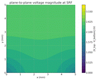
We treat these two 5 mm × 5 mm metal sheets (ABCD and A’B’C’D') as perfect conductors separated by a uniform dielectric of thickness t and relative permittivity εr. The plates are corner-fed at A and B′. We solved a frequency-domain model and plot the plane-to-plane voltage ΔV(x, y), which is proportional to the normal electric field in the dielectric (E ≈ ΔV/t). In sinusoidal steady state, the displacement-current density magnitude follows |Jd| = ω ε|E| ≈ ω ε|ΔV|/t, where ω = 2πf and ε = ε0 εr.
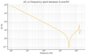
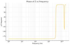
At first, ChatGPT generated a mesh model and calculated its impedance plot. And in this model, we have the self-resonant frequency (SRF) at 3.4GHz.
NOTE: Again, it’s qualitative information, not related to the physical MLCC device tested above.
Fig. 14– 14. ChatGPT5-assisted Model Impedance Plot, Gain |
Fig. 14– 15. ChatGPT5-assisted Model Impedance Plot, Phase |
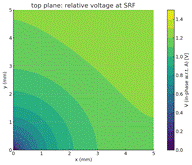
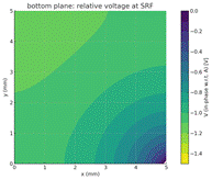
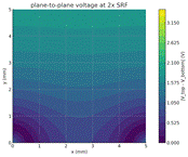
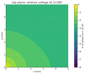
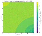
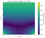
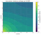
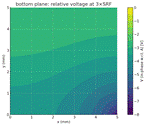
In table below, we have three rows for 1×SRF, 2×SRF, 3×SRF and we have three columns for (left) main plot of the displacement current density, (center) top plane relative voltage, (right) bottom plane relative voltage where difference between (center) and (right) resulting (left).
- At SRF, ΔV spreads broadly over the plane pair, indicating that a large portion of the area participates in displacement current, consistent with the minimum impedance.
- At 2×SRF and 3×SRF, interference patterns create inactive regions where ΔV is small, reducing the effective area and increasing impedance.
These in-plane modal patterns explain why #Case-3, which lacks a repeating Z-direction layer structure, does not exhibit the pronounced vertical standing-wave sequence seen in #Case-1 and #Case-2. In-plane modal patterns may still appear, but they do not produce the pronounced multi-peak behavior observed when the stack repeats in the Z-direction.
At Self-Resonant Frequency | ||
Fig. 14– 16. Plane-to-plane Voltage, ΔV |
Fig. 14– 17. Top Plane Relative Voltage |
Fig. 14– 18. Bottom Plane Relative Voltage |
At 2× Self-Resonant Frequency | ||
Fig. 14– 19. Plane-to-plane Voltage, ΔV |
Fig. 14– 20. Top Plane Relative Voltage |
Fig. 14– 21. Bottom Plane Relative Voltage |
At 3× Self-Resonant Frequency | ||
Fig. 14– 22. Plane-to-plane Voltage, ΔV |
Fig. 14– 23. Top Plane Relative Voltage |
Fig. 14– 24. Bottom Plane Relative Voltage |
This is the input to ChatGPT 5:
We have a pair of very thin metal foil sheets of 5mm x 5mm each, say sheet ABCD and sheet A’B’C’D', forming a capacitor with a tiny gap filled by a certain dielectric material. We attach a "drive" and "return" cable tips, from an AC signal source, at 2 corners of this capacitor, say A and B' (B-dash).
You can set reasonable parameters as you need here. Please calculate the impedance of this foil capacitor between A and B' over different frequency. We must have a self-resonant frequency and, at that self-resonant frequency, I want to see the "voltage distribution between ABCD and A’B’C’D' " and "current distribution through the dielectric" over the 5mm x 5mm sheet in 2D contour maps.
Please note that, at SRF, we expect A - B' voltage to be very small but large current flow across A - B'. With low voltage, dielectric never flow large current. So we expect large voltage between edge C-D and edge C' - D'.
When plotting impedance over frequency, please generate 2 plots: "abs(Z) in log-scale" vs freq, angle(Z) vs freq Lastly, please plot the same plane-to-plane voltage map at 2x SRF and 3x SRF.