

The current trend in the growing S-band market demands wider bandwidths, higher power levels and wider pulses, which are best served with a new technology to satisfy these advanced requirements. AlGaN/GaN HEMT on silicon substrate technology is a viable alternative to traditional technologies for high power transistors used in pulsed applications because of the lower thermal stress of pulsed operation compared to CW. The IGN2731M25 from Integra Technologies Inc. is the first in a series of devices designed for RF, pulsed power for S-band radar applications using GaN on a silicon substrate.

Figure 1 IGN2731M25 produces over 25 W from 2.7 to 3.1 GHz (32 V, 300 µs and 10% duty cycle).
The IGN2731M25 utilizes a 6 mm GaN HEMT chip on silicon substrate and is housed in an industry standard single-ended package (see Figure 1). The device has 50 µm gate-gate spacing and 100 µm gate finger length. Source pads are outside of the active area and connected to each source metal region by a dielectric overlay, i.e. no air bridge technology has been used. The semiconductor chips are 4 mils thick after wafer thinning, resulting in excellent thermal performance.

Figure 2 Output power and efficiency υs. input power for IGN2731M25.
RF characterization of the IGN2731M25 device was conducted with approximately 5 mA/mm of forward bias current and 32 V of drain bias. The device was characterized with pulsed input signal conditions with a 300 µs pulse width and 10 percent duty cycle. The device electrical characterization of the AlGaN/GaN HEMT is shown in Figure 2. The power drive-up curve shows output power performance exceeding 4 W/mm across the frequency band of operation between 2.7 and 3.1 GHz while exhibiting more than 50 percent efficiency in this range.

Figure 3 Gain and input return loss υs. input power for IGN2731M25.
The input return loss performance across power level and over frequency is shown in Figure 3. An input matching network has been implemented using a silicon MOSCAP and the inductance of the bond wires under the lid of the package. The device also has good isolation and is very stable with a 3:1 VSWR on the load.
Output power droop is a critical measurement parameter for system level performance. Figure 4 demonstrates the power droop from 2.7 to 3.1 GHz, which exhibits almost no droop, i.e. less than 0.25 dB even when the devices are saturated. Since power droop is typically attributed to heating, the demonstrated droop performance is another testament to the thermal performance of the GaN on silicon device geometry design.

Figure 4 Power droop υs. output power for IGN2731M25.
Existing GaN on silicon technology operates at 28 V, whereas GaN on SiC is available at both 28 and 50 V. Clearly 50 V operation with its higher power density capability is a much desired feature in the high power S-band radar market. The GaN HEMT technology processed on silicon versus the more expensive substrate material is attractive both from a current cost basis standpoint and the possibility of manufacturing on larger wafers.

Figure 5 Output power υs. frequency at Vdd = 32 and 48 V for IGN2731M25.
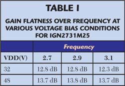
GaN on silicon technology for operation at 28 V is already standard; however, a robust AlGaN/GaN HEMT technology for operation at 50 V has not yet reached the market. The GaN HEMT process flow described earlier has been modified to include a major feature that improves RF performance in the S-band region: A gate connected field plate to improve breakdown and, therefore, operation at higher voltage. Although 50 V GaN on SiC solutions for S-band are available in the marketplace from several vendors, this device is the first GaN silicon technology operating at 50 V. This enhancement can be accomplished by using a dielectrically defined gate resulting in breakdowns well above 100 V and allowing 50 V operation. The higher operating voltage accounts for higher performance, as seen in Figure 5, where at a fixed input power of 3 W the device produces another 30 percent more power across the operating frequency band. Table 1 demonstrates how the gain parameter improves by more than 1 dB and gain flatness is negligible measuring 0.1 dB over 400 MHz from 2.7 to 3.1 GHz.
GaN HEMT technology has excellent power density and thus small parasitic die capacitance resulting in higher impedances for the designer to work with. The single stage input match results in more than 3 ohms of real impedance while the unmatched output stage has 5 ohms of real impedance, which contributes to the improved bandwidth response of the transistor (see Figure 6). The higher impedance facilitates the matching networks at the PCB level in a 50 ohm system.

Figure 6 Impedance υs. frequency for IGN2731M25.
Although this first generation technology demonstrates high performance, the GaN roadmap includes future designs with shorter gate lengths resulting in better frequency response and improved gain. The next generation targets 0.5 µm gate length, which is expected to have performance suitable for C-band applications.
The advantages of GaN technology serving several pulsed applications with small, high impedance, and reliable products addressing the radar and avionic bands are clear. As market demand grows and requires a new technology with higher voltages and broader bandwidths, additional RF power transistors will be developed that will continue to reduce system size, weight and cost leading to a host of new applications that can be served.
Integra Technologies Inc.,
El Segundo, CA
(310) 606-0855, www.integratech.com.
RS No. 304