
Communication systems today comprise the major use of GaAs technology with the highest volumes found in the cellular handset front-end. Here, heterojunction bipolar transistor (HBT) power amplifiers (PA) and Pseudomorphic High Electron Mobility Transistor (PHEMT) switches enjoy a comfortable market share. In this environment, the demands of production design require a robust CAD system with accurate and verified compact models for both active and passive devices. In this paper, we will outline some of the work done at RFMD® to develop and support scalable HBT models suitable for handset power amplifier design.
In the first section, a brief outline is given of the evolution of a custom HBT model from a basic Gummel-Poon formulation to one encompassing more GaAs physics. It is written in Verilog-A and and runs in multiple environments. In the second section, a model of a single device is shown that can be scaled to simulate the behavior of large output arrays. This will include both electrical and thermal aspects. Finally, we will present validation data to illustrate the performance of the model.

Figure 1 Cross-section of two-finger HBT (not to scale).
A cross-section of a simple two-finger HBT is shown in Figure 1. In these devices, the emitter is made of a wider bandgap material such as AlGaAs or InGaP while the base has a narrower bandgap, typically GaAs. In a single-heterojunction device, the base, collector and sub-collector will all be of the same material, while in a double-heterojunction bipolar transistor (DHBT) the collector will use a wider material. The energy band diagram for the more general DHBT is shown in Figure 2. In these systems, the potential barrier seen by base holes in the valence band is higher than that seen by emitter electrons in the conduction band. This results in higher emitter injection efficiency, leading to higher gain. In a conventional homojunction bipolar junction transistor (BJT), high injection efficiency requires a highly doped emitter and a thicker, lower doped base, increasing the base resistance and base transit time. The theory behind this dates back to the early days of the transistor.1

Figure 2 Energy band diagram of a HBT.
The HBT Model
DC Operation

Figure 3 Large-signal equivalent circuit for RFMD HBT model.
The large-signal equivalent circuit used in the model is shown in Figure 3. In typical fashion, we divide the device into intrinsic and extrinsic sections. To characterize the DC behavior, we need to develop expressions for the emitter-collector transport current (ICE) and the two base diodes that create it (IBE, IBCi). We begin with the Gummel-Poon formulation for the forward current2 (due to injection across the base-emitter junction).
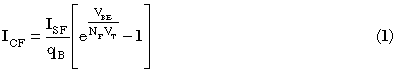
Here, qB is the hole charge in the base normalized to its equilibrium value (i.e., qB = QB/QB0.) Thus, at zero bias qB=1. Similarly, the reverse transport current is written as

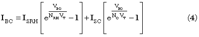
and the total current is simply the difference between the two: ICE=ICF-ICR. Note that we have used separate saturation currents (ISF, ISR) and ideality factors (NF, NR) for forward and reverse operation. In conventional silicon homojunction devices this is not necessary since the reciprocity principle ensures that both currents are equal for equal bias. In HBTs, however, the presence of conduction band spikes at the junctions can give rise to additional transport mechanisms such as thermionic emission and tunneling. If these are significant, we need the flexibility of the additional parameters. To illustrate this, consider the forward and reverse Gummel plot for a single-heterojunction AlGaAs/GaAs device, as shown in Figure 4 (a). In this technology, the emitter/base interface was graded to minimize the conduction band spike. The slope and intercept of the “ideal” part of the current is the same and could be modeled using one IS and N. Figure 4 (b), on the other hand, shows the same measurements for an InP DHBT. With conduction band spikes at both the emitter-base and base-collector junctions, the additional parameters are necessary.
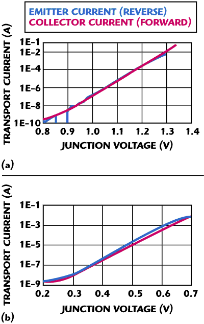
Figure 4 Forward and reverse collector-emitter current for a graded AlGaAs/GaAs single heterojunction (a) and an InP double heterojunction (b) transistor.

Figure 5 Forward beta-IC/IB (a) and reverse beta-IE/IB (b) for an AlGaAs HBT.
Similar flexibility is required in modeling the base current. The DC current gain of an HBT is nonlinear and cannot be written as the transport current divided by some beta parameter. Consider the plots of DC beta (forward and reverse) versus current shown in Figures 5 (a) and (b). Not only is there a large variation in gain, but the forward and reverse beta differs by two orders of magnitude. Thus, we use separate saturation currents and ideality factors for both ideal and leakage components:

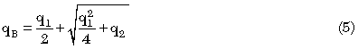
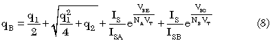
Next we consider the normalized hole charge qB. In the standard Gummel-Poon method, two effects are normally considered that will change the hole charge from its equilibrium value. The first is the Early effect3 in which the width of the un-depleted base changes with bias (Equation 6). The second is the high-current Kirk effect4 in which the base region can push out into the collector (Equation 7). The two effects are combined into Equation 5.
where

In HBTs with their highly-doped bases, the Early effect is not significant but we have left the parameters in mainly for nostalgia. There are, however, a variety of high-current effects. Using this formulation, the high current limit of ICE tends to
(i.e., a fixed ideality factor of 2.0). For HBTs we need more flexibility and thus we add an additional expression to qB, similar to the one used in the Agilent HBT model.5
Temperature Modeling
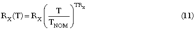
The most common approach to temperature modeling is to make some subset of the parameters functions of either a ratio or difference of the junction temperature to some reference temperature, e.g., X(T)=f(T/TNOM) or X(T)=f(T-TNOM). Some can be physics-based while others are purely phenomenological expressions. For example, the variation of saturation current is usually modeled as
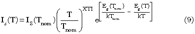
This equation can be derived from the power law temperature variation of the conduction and valence band effective density of states. In contrast, the ideality factors are written simply as

And parasitic resistances is written as
Charge Expressions - QBE
All capacitances in our model are written as charge expressions and implemented using the Verilog-A ddt() operator. The base-emitter junction has three terms associated with it: The depletion region junction capacitance, a diffusion capacitance associated with the base transit time and a charge to account for the high-current Kirk effect.
The junction capacitance is modeled using the usual expression
where the corresponding charge is just the integral over voltage.
The narrow, highly doped base of an HBT allows us to model the diffusion charge simply as a constant transit time multiplied by the forward transport current:

Finally, the Kirk effect is modeling using a power-law-based transit time
The resulting base-emitter charge term is simply the sum of all three effects

Charge Expressions - QBC
In the base-collection junction, the reverse-bias depletion capacitance is limited by the width of the collector, as the depletion region width will not change significantly once it reaches the sub-collector. To account for this effect, Equation 12 needs to be modified in some way. In our work, we have adopted the approach used in HICUM Level 0, as it is simple to implement and simple to extract.6
The time constant associated with the collector delay has a forward current dependence that is modeled with a hyperbolic tangent function after Iwamoto7

A base diffusion capacitance is also incorporated due to the reverse transport current and writes the base-collector charge as a sum of these terms:

HBT Self-Heating
HBTs used in PA applications are run at relatively high power densities. Thus, the Joule heating in the device can lead to a significant temperature rise. This is illustrated in Figure 6. The DC beta of an AlGaAs/GaAs device decreases at higher temperatures, and this drop can be seen in the forward IV curve, especially in the regions where power dissipation is high. We model this effect in the most common way, which is to approximate the various thermal time constants in the structure by a two-pole lumped element circuit driven by a current source. The value of the current is set equal to the power dissipated in the device (usually dominated by the drop across the base-collector junction). The voltage developed across the current source is equal to the device temperature rise that is fed back into the temperature model to solve for the device current in a consistent manner until the electrical simulation converges. We provide external pins for both sides of the thermal circuit. The “bottom” pin can be connected to an external thermal network that represents a package while the upper node can be attached to another network to simulate thermal coupling. The resulting five-terminal equivalent circuit is shown in Figure 7. In the thermal network of Figure 7, Cth, Rth2 and Cth2 are constant parameters of the model, while the Rth element is temperature dependent.
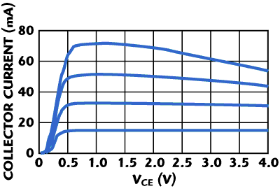
Figure 6 Forward I-V measurement of an AlGaAs/GaAs HBT showing the effects of self-heating.

Figure 7 Five-terminal large-signal equivalent circuit incorporating two-pole self-heating.
In early works, the thermal resistance of an HBT was constant and most commonly extracted with Dawson’s procedure.10 Yeats11 provided a more rigorous expression for thermal resistance as a function of ambient temperature and dissipated power. This approach is necessary to account for the temperature-dependant thermal conductivity of GaAs; however, there was a concern over potential numerical issues as Yeats’ parameter n is close to 1, and (n-1) is in a denominator. Yeats’ parameter n comes from the expression for the temperature dependence of thermal conductivity.
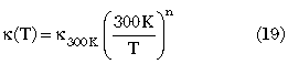
Since n is typically close to 1, this implies that the thermal resistively is approximately linear in temperature. Therefore, we adopted a linear-temperature dependence in the expression for thermal resistance.
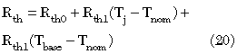
The model parameters are Rth0 and Rth1; Tj, Tbase and Tnom are the junction, device-base and nominal-model temperatures, respectively. The formula in Equation 20 makes the thermal resistance in effect dependent on the thermal gradient from the junction to the base of the transistor (node TB in Figure 7). It is worth noting that we investigated separate parameters for the Tj and Tbase contributions in Equation 20, but found that it had no practical benefit.
Akin to the approaches in References 10 and 11, the thermal resistance parameters are determined by fitting the base-emitter voltage versus dissipated power at a constant emitter current, Equation 20 coupled with the following:
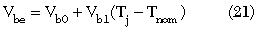
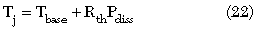
Figure 8 shows the fit of the thermal resistance model to measurements on a standard transistor cell. This same data set was fitted to Yeats’ thermal resistance equation in Reference 11. Figure 9 compares the thermal resistance of our model to that of Yeats’ formula versus junction temperature with a 25°C base temperature. The agreement is quite good over the junction temperature range expected in normal operation (in this case less than 100°C) and shows that the simplification of the model provides sufficient accuracy while avoiding potential stability or convergence problems. Lastly, it should be noted that some other models do have temperature-dependent thermal resistances.8,9 Unfortunately, these models only take into account the junction temperature, thus ignoring the effect of any thermal gradient in the device substrate.
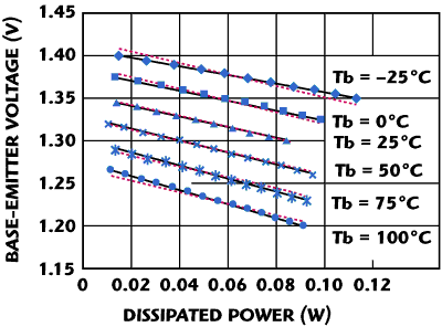
Figure 8 Measured (symbols), modeled per this article (solid lines) and modeled with constant thermal resistance value (dashed lines) base-emitter voltage vs. dissipated power for a single-cell HBT (32 mA).
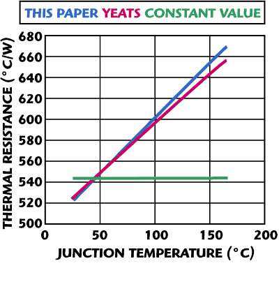
Figure 9 Calculated thermal resistance vs. junction temperature for various models.
Returning to the four elements of the thermal circuit (Rth2, Cth2, Rth and Cth), typically Rth2 and Cth2 are set to small, negligible values. Rth and Cth are extracted based on the methods presented in References 10 and 12 and the discussion of the previous paragraph. The thermal resistance extraction methods assume that if a constant emitter current (high enough to observe significant power dissipation) is forced through the device then the variation in base-emitter voltage is only due to the variation in junction temperature. Measurements are conducted over a wide range of temperatures to account for the temperature dependence of thermal resistance. The thermal capacitance is extracted from pulsed I-V measurements using the normalized difference unit (NDU) method.12 The method is based on the comparison of pulsed I-V measurements of different pulse lengths to static I-V measurements. The thermal time constant is defined as the time after a step in Pdiss when 63.2 percent of the resulting change in the junction temperature has occurred. From the NDU versus pulse length plot, the thermal time constant (tau) is extracted (see Figure 10) and the thermal capacitance is calculated as
Unlike the thermal resistance, the thermal capacitance is assumed to be temperature independent.
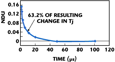
Figure 10 Extraction of the thermal time constant from the NDU vs. pulse length.
Single Cell Model Validation
Once extracted, a transistor model should be validated in multiple ways. Our HBT model is fully checked against DC measurements and S-parameter measurements over a wide range of biases and temperatures. This verifies that the model plays back the types of measurements used in the model extraction. Once the extracted model shows good agreement with this first-step validation, a second level of validation is performed with on-wafer large-signal measurements such as 50 Ω power sweeps,13 source/load-pull measurements and waveform measurements.
The 50 Ω power sweep is performed with a commercial vector network analyzer (VNA), which is calibrated to measure vector S11 and S21 as well as the power at second and third harmonics. Measurements in the 50 Ω power sweep setup are done over bias and temperature. Even though the load-line for this measurement is 50 Ω, through a combination of biases and power levels, the device is effectively exercised over its full I-V plane. Since this measurement can be easily integrated into the same measurement stand that performs on-wafer, DC and S-parameter measurements, it is a valuable first-step in large-signal validation. Figures 11 (a) and (b) show a comparison of the measured and simulated output power at the fundamental, second harmonic and third harmonic from 50 Ω power sweeps at a Class A and Class AB bias point, respectively. Because of the flexibility to cover multiple test conditions with the 50 Ω power sweep, we have devised a metric (discussed in Reference 13) that gauges the relative error between the simulation and the measurement. This metric has been very helpful in judging the improvements in the model as it evolved to its present form.
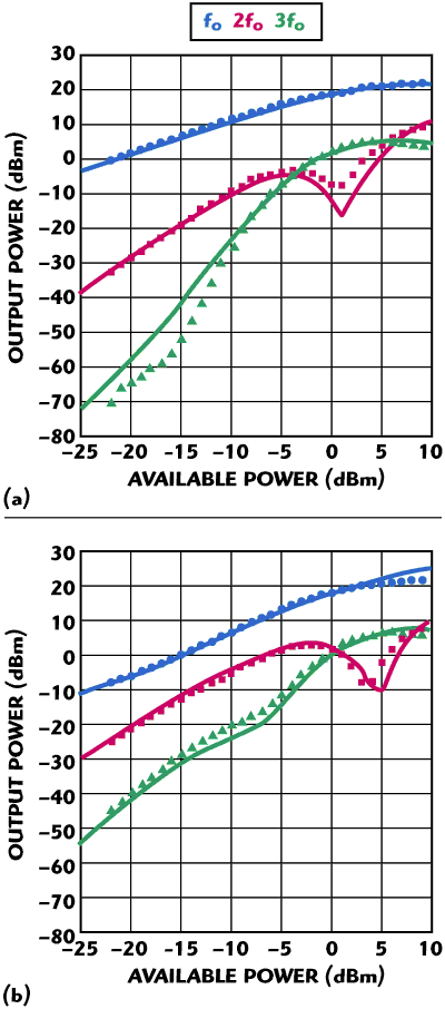
Figure 11 Measured (symbols) and simulated (solid lines) output powers at ƒ0, 2ƒ0 and 3ƒ0 from a 50 Ω power sweep on a single HBT at Vc=3.5 V and Icq=20 mA (a) and Icq=2 mA (b).
Waveform measurements are also performed on-wafer at ambient temperature, and for this measurement we use a commercial large-signal network analyzer (LSNA). The spectral components of the base and collector voltages and currents are measured at the transistor reference plane, and the time domain waveforms are calculated. The system is configured to vary bias and RF drive power as well as the input and output impedances using mechanical tuners. Figures 12 (a) and (b) show the base and collector waveforms at a Class AB bias point for nominal 50 Ω source and load terminations.
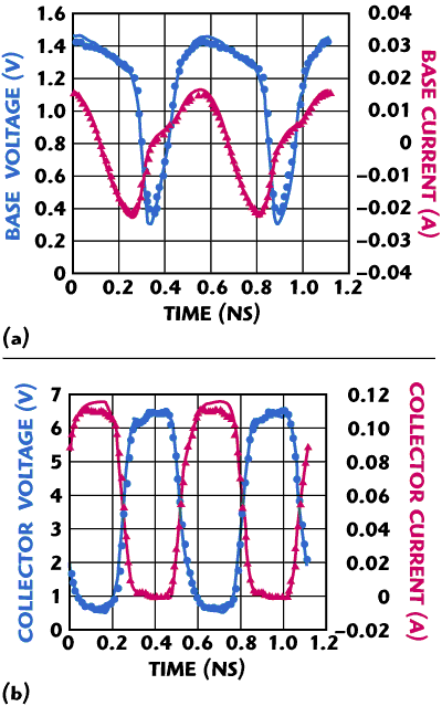
Figure 12 Measured (symbols) and simulated (solid line) base (a) and collector (b) voltage and current waveforms with nominal 50 Ω loading (Vc=3.5 V, Icq=2 mA and Pavs=5 dBm).
Multi-cell Array Modeling
In PA applications, scaling the model from a single device to large arrays is necessary. Using a simple multiplication factor is not sufficient, as the parasitic interconnect and thermal behavior of an array will be quite different from the single cell transistor used to extract the model.
Our approach for multi-cell array modeling involves a combination of EM simulations of the interconnect manifolds and scaling of the thermal impedances14 to account for the increase in operating temperature due to the proximity of devices in the array. While the manifold modeling is handled using EM simulation,14 thermal modeling of the arrays is implemented in two different ways:
- Deriving a custom thermal impedance scaling equation in the Verilog-A code that is capable of predicting the average junction temperature for various array layouts, and
- Adding thermal coupling networks between the thermal nodes (utilizing the TH and TB pins of Figure 5 (b)) of neighboring devices without altering the internal thermal resistance.
A custom thermal scaling equation or a thermal coupling network can be generated in many different ways;15-20 for example, by using a finite-difference numerical thermal simulation,21,22 by using a 3-D finite-element steady-state thermal solver23,24 or by optimizing to achieve a best fit with measured data (I-V curves).15,17
For the first approach where it is necessary to derive a thermal scaling equation that provides an average temperature for a variety of layouts, we started from electrical measurements extracting effective, average thermal resistances for arrays with different numbers of cells and cell-to-cell separations. The equation consists of the thermal resistance of a single cell and a correction function to account for the number of cells and the cell-to-cell separation.

Rth_nom is the thermal resistance of a single cell device, N is the number of cells and y is the device pitch. The function, ƒ(N,y), simply modifies the thermal resistance function of an isolated device, scaling it by an array-specific factor. The unit-cell thermal resistance in Equation 24 is already temperature-dependent and is separately scalable with respect to within-cell geometry. The function, ƒ(N,y), is derived empirically for arrays of selected unit cells by curve-fitting to the measured DC data until the best fit to the overall array I-V characteristics is achieved. The thermal scaling equation is then validated against TCAD simulations at low- and medium-power dissipations (see Figure 13).
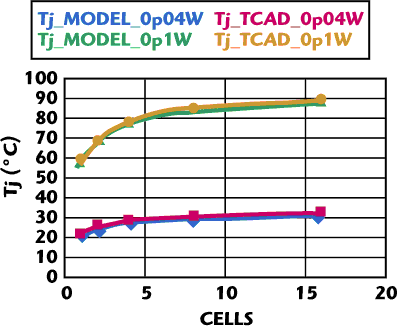
Figure 13 Comparison of modeled and TCAD-simulated Tj as a function of cell number (Pdiss=0.04 and 0.1 w/cell).
To extend the scaling equation to arrays of a larger variety of unit cells, TCAD simulations were employed. TCAD simulations of array temperatures provide a low-cost, efficient alternative to generating data from electrical measurements on real arrays. After the initial calibration of the simulation to measured results, TCAD is used to generate a large set of thermal data from which we derive the scaling function for each unit cell type. Because the TCAD input decks are typically text files, it is straightforward to write a script that automatically generates input decks for arbitrary arrays of unit-cell power sources arranged in a regular grid. This automated deck generation along with the short TCAD simulation times allowed for the efficient creation of large sets of thermal data (see Figure 14).
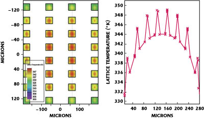
Figure 14 Layout generated TCAD with temperature imbalance in an array.
In this first implementation of Rth modification for arrays, the array is represented as a collection of identical parallel HBTs where each device has an “average” thermal resistance that yields the effective array temperature at a given power dissipation. Thus, there is no temperature or electrical variation from cell to cell within the array. Instead, each device has a modified thermal resistance that effectively increases the device temperature at a given Pdiss compared to an isolated device running at the same Pdiss. Since this approach provides an average junction temperature, it cannot be used to analyze the “hot spots” in the array caused by any thermal imbalance. Although this approach does not provide information about the temperature distribution in the array, in many cases it is desirable to use this simplification as it results in shorter simulation times and improved robustness due to fewer electrical nodes without impacting simulation accuracy.
The second approach for the thermal modeling of multi-cell arrays is based on creating a network of thermal resistances connecting adjacent devices. This allows devices within an array to have distinct temperatures, thus giving a more accurate prediction of the temperature distribution in the array at the expense of simulation time and complexity. Thermal resistors are used to connect the thermal nodes of the five-terminal model for adjacent devices, as shown in Figure 15. The heat paths represented by the resistive network are shown in Figure 16.
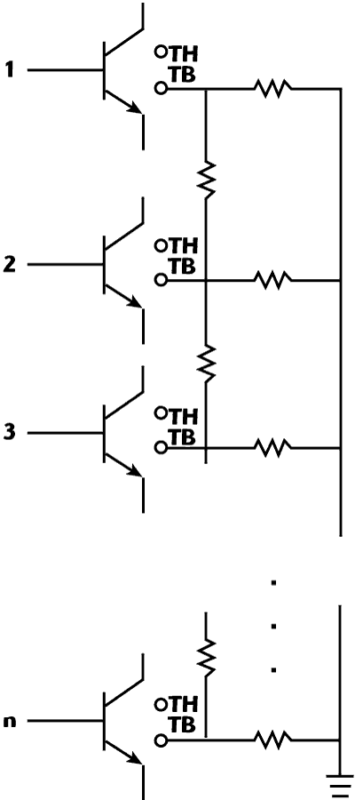
Figure 15 Thermal coupling network to account for thermal imbalance in an array.

Figure 16 Heat dissipation in multi-cell device.
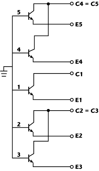
Figure 17 Test structure used to evaluate neighbor heating for the thermal coupling network.

Figure 18 Modeled (symbols) and measured (solid lines) emitter voltage and junction temperature of a two-cell device (device 1 is turned on while device 2 emitter current is swept).
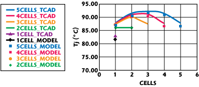
Figure 19 TCAD (lines) and model (symbols) simulations of Tj (Pdiss=0.1 w/cell, Tamb=25°C).
In our approach, we adopt a simplified pi-network where the resistances are extracted using a test structure, as shown in Figure 17. The values of the thermal resistors used to connect adjacent devices can be derived from electrical measurements that represent a change in an individual device’s temperature as its neighbor devices are individually powered on (see Figure 18). This is again based on the Vbe thermometer method, inferring a temperature rise in a given device as a neighbor heats it from the change in Vbe needed to produce a constant emitter current. Test data shows that the temperature rise due to thermal coupling is proportional to the power dissipated in the neighboring transistors and depends on the proximity of the neighbor transistors with the device under test. Results were validated by comparing the electrical simulation of a two-cell through five-cell array with thermal coupling networks to TCAD simulation (see Figure 19). Utilizing the results from this test, we were able to generate thermal coupling networks for larger arrays using the principle of superposition, where the thermal resistors are calculated from a device’s temperature rise attributed to power dissipated by its nearest neighbors. The approach was tested for a variety of device spacing, array configurations and cell numbers. It is important to note that the thermal coupling networks are extracted from measurements done at room temperature, relying on the fact that intrinsic thermal resistance is temperature-dependent. If higher accuracy is desired over a wide temperature range, it would be necessary to assign temperature-dependence to the elements in the thermal network.
For the full validation of a multi-cell array model, we consider a more practical example, a typical 32-cell array. While either approach for the thermal modeling can be used, the first approach described above has been used for this example. The results are shown in Figures 20 and 21, where the measured data is marked by circles with the simulation by a solid line. Figure 21 (a) and (b) indicate a reasonable match to ΓIN with the power gain within 0.7 dB over 6 dB into compression. Figure 21 (c) shows the power added efficiency (PAE) with less than 5 percent error. Finally, the measured versus simulated dynamic load line is shown in Figure 21 (d).

Figure 20 I-V curves for large arrays generated using a principal of superposition at -25°C (a), 25°C (b) and 85°C (c).

Figure 21 Thirty-two-cell model validation: Input Gamma vs. available power (a), power gain vs. available power (b), PAE vs. available power (c) and dynamic load line (d).
Conclusion
We have discussed the salient features of a custom III-V HBT model and its scaling for cellular PA applications. While this custom model is similar in basic accuracy at the unit-cell level to some commercially available models, we have found the flexibility to tailor a custom model to an application space beneficial to scaling the model to multi-cell arrays used in product designs without degrading array-level accuracy or simulation time.
Acknowledgments
We wish to thank F. Kharabi, B. Clausen, S. Parker, P. Li, T. Dinh, E. Davis and D. Halchin for many varied and helpful discussions. Also, we wish to thank L. Hill, D. Wernsing, G. Lyons, C. Lineberry, H. Randall, T. Howle, A. Harman and S. Dorn for support with the measurements and keeping our feet on the ground. Lastly, we wish to thank A.J. Nadler for reviewing our manuscript and RFMD for supporting this effort.
References
- H. Kroemer, “Theory of a Wide-gap Emitter for Transistors,” Proceedings of the IRE, Vol. 45, No. 11, 1957, pp. 1535-1537.
- H.K. Gummel and H.C. Poon, “An Integral Charge Control Model of Bipolar Transistors,” Bell System Technical Journal, Vol. 49, 1970, p. 827.
- J.M Early, “Effects of Space-charge Layer Widening in Junction Transistors,” Proceedings of the IRE, v40, 1952, p. 1401.
- C.T. Kirk, “A Theory of Transistor Cutoff Frequency (fT) Falloff at High Current Densities,” IRE Transactions on Electron Devices, v9, n2, 1962, pp. 164-174.
- Agilent Heterojunction Bipolar Transistor Model, Agilent Advanced Design System Documentation 2008, Nonlinear Devices Chapter 2, pp. 4-33.
- M. Schroter, S. Lehmann, H. Jiang and S. Komarow, “HICUM/Level0 – A Simplified Compact Bipolar Transistor Model,” IEEE Proceedings of the 2002 Bipolar/BiCMOS Circuits and Technology Meeting, 2002, pp. 112-115.
- M. Iwamoto, D.E. Root, J.B. Scott, A. Cognata, P.M. Asbeck, B. Hughes and D.C. D’Avanzo, “Large-signal HBT Model with Improved Collector Transit Time Formulation for GaAs and InP Technologies,” IEEE International Microwave Symposium Digest, 2003, pp. 635-638.
- Agilent Heterojunction Bipolar Transistor Model, Non-Linear Devices, Agilent ADS Documentation v2005A, Chapter 2, 2005, pp. 4-42.
- UCSD HBT Model, http://hbt.ucsd.edu.
- D.E. Dawson, A.K. Gupta and M.L. Salib, “CW Measurement of HBT Thermal Resistance,” IEEE Transactions on Electron Devices, Vol. 39, No. 10, October 1992, pp. 2235-2239.
- B. Yeats, “Inclusion of Topside Heat Spreading in theDetermination of HBT Temperatures by Electrical and Geometrical Methods,” 21st Annual Gallium Arsenide Integrated Circuit Symposium Digest, October 1999, pp. 59-62.
- C. Baylis, L. Dunleavy and J. Daniel, “Direct Measurement of Thermal Circuit Parameters Using Pulsed IV and Normalized Difference Unit,” Microwave Symposium Digest, 2004 IEEE MTT-S International, Volume 2, June 2004, pp. 1233-1236.
- J. Gering, S. Nedeljkovic, F. Kharabi, J. McMacken and D. Halchin, “Transistor Model Validation through 50 Ohm, Vector Network Analyzer Power Sweeps,” 70th ARFTG Conference.
- S. Nedeljkovic, J. McMacken, J. Gering and D. Halchin, ”A Scalable Compact Model for III-V Heterojunction Bipolar Transistors,” Microwave Symposium Digest, 2008 IEEE MTT-S International, June 2008, pp. 479-482.
- H. Beckrich, S. Ortolland, D. Pache, D. Celi, D. Gloria and T. Zimmer, “Impact of Neighbor Components Heating on Power Transistor Electrical Behavior,” Microelectronic Test Structures, 2006 IEEE International Conference, March 2006, pp. 205-210.
- D. Walkey, T.J. Smy, D. Celo, T.W. MacElwee and M.C. Maliepaard, “Compact, Netlist-based Representation of Thermal Transient Coupling Using Controlled Sources,” IEEE Transactions on Computer-Aided Design of Integrated Circuits and Systems, Vol. 23, No. 11, November 2004, pp. 1593-1596.
- P. Dai, P. Zampardi, K. Kwok, C. Cismaru and R. Ramanathan, “Study of Thermal Coupling Effect in GaAs Heterojunction Bipolar Transistor by Using Simple Mirror Circuit,” GaAs ManTech 2005.
- D. Walkey, T.J. Smy and D. Celo, ”Prediction of Maximum Temperature Rise in Multi-finger Transistor Structures Using Normalization,” GaAs ManTech 2002.
- P. Baurelis, “Electrothermal Modeling of Multi-emitter Heterojunction Bipolar Transistors (HBT),” Integrated Nonlinear Microwave and Millimeter-wave Circuits Third International Workshop, October 1994, pp. 145-148.
- M. Schubler, V. Krozer, J.G. de la Fuente and H.L. Hartnagel, “Thermal Coupling in Multi-finger Heterojunction Bipolar Devices,” 27th European Microwave Conference and Exhibition, September 1997, pp. 104-108.
- D. Denis, C.M. Snowden and I.C. Hunter, “Coupled Electrothermal, Electromagnetic and Physical Modeling of Microwave Power FETs,” Microwave Theory and Techniques, IEEE Transactions, Vol. 54, Vol. 6, June 2006, pp. 2465-2470.
- M. Rudolph, F. Schnieder and W. Heinrich, “Investigation of Thermal Crunching Effects in Fishbone-type Layout Power GaAs-HBTs,” Gallium Arsenide Applications Symposium GaAs 2004, October 2004, Amsterdam, The Netherlands.
- H. Beckrich, T. Schwartzmann, D. Celif and T. Zimmer, “A Spice Model for Predicting Static Thermal Coupling Between Bipolar Transistors,” Research in Microelectronics and Electronics, 2005 PhD, Vol. 2, July 2005, pp. 75-78.
- D. Lopez, R. Sommet and R. Quéré, “Spice Thermal Subcircuit of Multi-finger HBT Derived from Ritz Vector Reduction Technique of 3D Thermal Simulation for Electrothermal Modeling,” Gallium Arsenide Applications Symposium GaAs 2001, 24-28 September 2001, London, England.
- A. Cidronali, G. Collodi, C. Accillaro, C. Toccafondi, G. Vannini, A. Santarelli and G. Manes, “A Scalable PHEMT Model Taking into Account Electromagnetic and Electro-thermal Effects,” Gallium Arsenide Applications Symposium GaAs 2003, 6-10 October 2003, Munich, Germany.