

A key advancement is the adoption of on-chip differential circuit topologies, eliminating the need for large, costly off-chip baluns traditionally used to convert single-ended RF paths to the converter’s differential interfaces. Implementing the filter as a differential design yields lower loss, improved common-mode rejection and a simplified layout, often requiring fewer board layers and interconnects. When implemented as a standardized building block across array elements, this approach delivers substantial SWaP-C benefits. This technology supports agile frequency tuning, high IIP3 (> 40 dBm typical) and compact die sizes, enabling co-location or direct interfacing with multi-channel converters in direct RF architectures.
Front-End Hardware Implementation
In the RF front-end of advanced wideband phased array systems, highly integrated modules will now incorporate the power amplifier (PA), low-noise amplifier (LNA), transmit/receive (Tx/Rx) switch, tunable filters and phase/gain control elements to enable full beamforming functionality. This level of integration minimizes interconnect losses, reduces parasitic effects and simplifies array tiling, calibration and thermal management. For wideband applications requiring large instantaneous bandwidths (2 to 18 GHz systems) or physically large arrays with wide scan angles, true time delay (TTD) architectures are increasingly employed in place of, or alongside, traditional phase shifters. TTD eliminates beam squint (frequency-dependent beam-pointing errors) by providing a constant group delay across the band, thereby preserving beam shape and directivity during wideband operation. This is key to maintaining high-resolution performance in contested spectra.
Achieving optimal SWaP-C performance in these applications often requires leveraging multiple IC technologies rather than relying on a single process. Hybrid approaches allow designers to assign high-power, high linearity functions to the most suitable material while using cost-effective, highly integrable technologies for lower-power or control-oriented blocks.
For example, GaN-on-Silicon (GaN/Si) technology is transforming transmit-chain performance by delivering higher output power than pure silicon-based solutions at lower cost than traditional GaN technologies. GaN/Si balances performance and cost, offering high power density, efficiency and breakdown voltage for broadband PAs, while leveraging large-diameter (200 mm) silicon wafers, CMOS-compatible processing and lower substrate costs. These attributes make GaN/Si well suited for scaling to dense, high EIRP arrays where thermal and power constraints are critical.
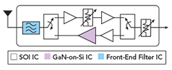
Fig 7. Front-end multi-chip module diagram.
Alongside the GaN/Si PA, low-cost SOI technology is well suited for tunable filters, transmit/receive switching and other low-power RF components. It offers sharp selectivity, fast digital tuning, high linearity and consistent inter-channel performance in compact chip sizes. These heterogeneous front-end ICs, with GaN/Si for power amplification and SOI for filtering/control, are then co-packaged or multi-chip integrated into a single, compact module (Figure 7). This multi-die module mounts directly onto the phased array antenna board (i.e., as a tile- or element-level TRM), providing a complete, self-contained RF module with all necessary functionality. This setup greatly reduces board size, assembly cost and overall weight and power, while maintaining the wideband agility and beamforming accuracy needed for next-generation systems.
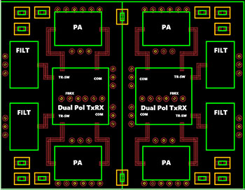
Fig 8. Front-end multi-chip module layout example.
Integrating these devices together, of course, presents its share of challenges. There are many factors to consider when integrating several ICs, such as how close they can be placed together, how to remove heat from the finished package (from the top of the ICs or the bottom of the part through the next higher assembly), which bump materials are used and whether they are compatible during the reflow process for flip-chipped parts, to name a few, see Figure 8.
It requires careful management of these items by the design team and generally involves several build attempts to refine the assembly process and ensure a high yield. Managing the coefficient of thermal expansion (CTE) mismatch across all materials involved is crucial to designing for high reliability and to ensuring that stresses at the various interfaces are well managed for long-term functionality. Working closely with the packaging and assembly vendors from the beginning is crucial to ensuring success.
Conclusion
As wideband phased array systems continue to evolve, the convergence of direct RF sampling, SOI-based tunable filters and heterogeneous front-end integration enables next-generation electromagnetic superiority. The architectural simplifications achieved through direct sampling directly address the core challenges of ultra-wide instantaneous bandwidths, dense spectral environments and stringent SWaP-C constraints in platforms ranging from airborne EW suites to satellite payloads and multi-function arrays.
Looking ahead, these technologies will accelerate the transition to simultaneous multi-domain operations. SOI tunable filters will increasingly replace bulky switched filter banks. This shift enables finer-grained agility in contested spectra, where rapid retuning can nullify frequency-agile jammers, excise narrowband interferers or maintain anti-aliasing protection across multi-GHz IBWs, all while preserving the phase/amplitude consistency essential for digital beamforming.
Heterogeneous integration will play an even more central role. Pairing high-power, high-efficiency GaN-on-Silicon (GaN/Si) PAs with SOI for tunable filtering enables compact, tileable transmit/receive modules (TRMs). The broader trajectory points to deeper levels of system-in-package and 3D heterogeneous integration, potentially incorporating advanced packaging techniques to enable ultra-low-latency processing.
The defense technologies underpinning these advances are also relevant to the emerging 6G FR3 ecosystem, spanning approximately 7 to 24 GHz. GaN-on-Silicon PAs and SOI tunable filters developed for EW and radar applications align directly with Frequency Range 3 front-end requirements, enabling dual-use convergence that will accelerate process maturation and reduce costs across both markets. This hardware foundation further positions the industry well for integrated sensing and communication (ISAC) architectures, in which a single wideband front-end simultaneously supports high-throughput data communication and active sensing functions such as radar and localization. SOI tunable filters and heterogeneous front-end modules, originally designed for multi-function EW platforms, are a natural fit for the linearity, filtering and instantaneous bandwidth demands that ISAC places on the RF front-end.
Integrating legacy discrete architectures with software-defined, digitally intelligent RF hardware, SOI-enabled tunable filtering and heterogeneous integration will remain essential to achieving electromagnetic dominance across air, sea, land, space and cyber domains in the coming decades. Ongoing investment in process refinement, packaging innovation and multi-domain co-design will further enhance performance, enabling cognitive and multi-function RF systems that expand the possibilities in EW and related fields.