

A wideband multilayer artificial magnetic conductor (AMC) structure comprises five periodic patch layers printed on different dielectric substrates with varying dielectric constants. The AMC structure is used as a ground plane for a printed wideband antenna to improve its gain. Over a 4.5 to 7.5 GHz 10 dB impedance bandwidth, its average gain exceeds 8 dBi with a maximum gain of 12 dBi.
In recent years, wideband antenna design has been a research focus with the rapid development of modern wireless communications.1 Many designs have been proposed, such as a quasi-Yagi antenna that can have a 75 percent impedance bandwidth2 and an L-probe feed patch antenna that can achieve an impedance bandwidth of 36 percent.3 The gains of these antennas, however, are not very high, which limits their application.
To address this, much attention has been focused on metamaterials for metasurfaces,4,5 lenses,6 frequency selective surfaces (FSSs)7 and AMCs.8-12 For the AMC structure, a plane wave is reflected in-phase (between -90 and +90 degrees) rather than out-of-phase, as occurs on the surface of a perfect electrical conductor (PEC). Since the reflected phase of an AMC does not cause destructive interference between direct and reflected waves, many researchers have adopted it to improve antenna gain and directivity.
Scarborough et al.8 employed an E-plane coupled closely-packed microstrip patch array loaded with a group of mushroom-like electromagnetic band gap (EBG) structures to effectively decrease lateral and backward radiation patterns by 13.19 dB and 7.76 dB, respectively. Mushroom-like structures can be considered as AMCs to replace the ground plane of an antenna to improve antenna gain and directivity.13-15 However, for the mushroom-like structure, which provides shorted left-handed stub inductors through metallic via holes, large currents concentrated around the vias generate considerable loss, which degrades gain and radiation efficiency.16 Fabrication of the structure is complex as well, increasing the antenna cost.
To decrease electromagnetic loss and simplify fabrication, the use of periodic patch-like mushroom structures has been attempted, named by some as patch-type AMC structures,16-19 which have the same characteristics of in-phase reflection as mushroom-like structures and are insensitive to the electromagnetic wave incident angle.20 However, because the AMC surface operates as a resonant mechanism, an antenna loaded with a monolayer AMC surface often exhibits a narrow bandwidth, which limits its practical application.
In this work, alternative and improved strategies are explored to address wideband gain enhancement. First, a new design methodology for constructing a multilayer AMC structure is introduced to broaden the in-phase reflection bandwidth. By using different dielectric constants and optimized patch sizes, the in-phase reflection bandwidth is significantly increased. Next, a wideband planar antenna with an impedance bandwidth from 3.8 to 7.5 GHz is designed. Finally, the multilayer AMC structure is employed as the antenna’s ground plane to enhance gain.
Prototype antenna measurements confirm the multilayer AMC’s performance. Due to the wideband in-phase reflection characteristics of the AMC, the antenna’s average gain is significantly improved to greater than 9 dBi from 4.5 to 7.5 GHz, peaking at 12 dBi.
MULTILAYER AMC STRUCTURE
The in-phase reflection bandwidth of the AMC surface is a design focus issue, important for its application. To expand the bandwidth, the phase property is investigated. Although numerical experimental data through parametric analysis has been provided,9 the theoretical basis is not adequate. Theoretical analysis of the reflection phase is given in detail here.
Assuming the incident wave penetrates on AMC surface, the phase delay Φd through the AMC structure is determined by calculating the ratio of the reflected (bn) and incident (an) fields and is calculated with Equations 1 through 5:
Where, τ1, τ2 and ρ1, ρ2 are the intrinsic transmission and reflection coefficients, respectively; η0 and η are the intrinsic wave impedances of the air and dielectric regions, respectively; τ is the thickness of the substrate; εr is its dielectric constant and k and λr are the wave number and wavelength in the dielectric, respectively. By simplification, the phase delay in the AMC structure can be calculated with Equations 6 and 7:
The patch-type AMC structure at resonance is equivalent to an LC parallel resonant circuit. The structure resonates within the frequency range where high impedance and in-phase reflection are met. The surface impedance of the patch structure is formulated in Equation 8:
Where C and L are the equivalent capacitance and inductance given by Equations 9 and 10, respectively, determined by the patch width a, gap g, the thickness t and the permittivity of the substrate.21
The phase characteristic is mainly determined by the dielectric constant εr and the thickness τ. The size of the patch also has some effect. To broaden the bandwidth of the in-phase reflection, the thickness of the substrate can be changed. However, if the substrate is too thick to be found in nature, it cannot be applied. Dielectric loss should be considered at microwave and higher frequencies as well.
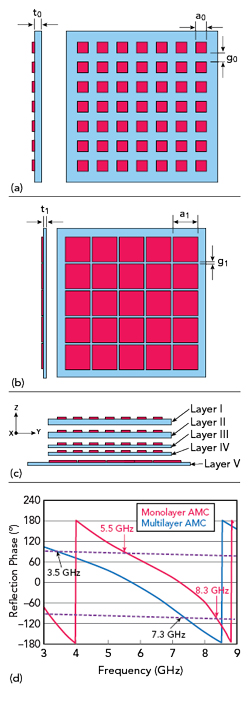
Figure 1 Multilayer AMC structure: top view of layer I to layer IV (a), top view of layer V (b), side view of the multilayer AMC structure (c) and reflection phase characteristics of monolayer and multilayer structures (d).
Another way of changing the dielectric constant is considered. In this work, a multilayer AMC structure is proposed. On one hand, a different dielectric constant for each layer is used to change the effective dielectric constant and broaden the bandwidth of in-phase reflection. On the other hand, the overall thickness is also changed with the multilayer structure. Furthermore, as air is filled between the layers, dielectric loss is greatly reduced.
The multilayer AMC structure consists of five layers (see Figure 1). The patches on the top two layers (Layers I and II) are constructed on FR-4 (εr = 4.4) with thickness τ0 = 1 mm, and the other patches (on Layers III, IV and V) are printed on Rogers (εr = 3.5) with thickness τ1 = 0.8 mm. The array of 7 × 7 square metallic unit cell patches for Layers I, II, III and IV all have the same dimensions.
An array of 5 × 5 metal unit cell patches for Layer V is designed with the patch width changed from a0 to a1, and the gap changed from g0 to g1. To expand the in-phase bandwidth, the parameters a0, a1, g0 and g1 are optimized to obtain an equivalent C and L that makes the phase and impedance vary slowly with frequency. Through numerical simulation, the parameters are optimized to a0 = 4.8 mm, a1 = 15 mm, g0 = 4 mm and g1 = 2 mm. The space between each layer of the multilayer structure is 2 mm.
For comparison, the reflection phase of a monolayer AMC structure is analyzed as well. For consistency, the thickness of the monolayer substrate τ =13.6 mm, which is the same as the height of the multilayer AMC. The patch width and the gap between adjacent patches in the monolayer substrate are the same as those of the top four layers of the multilayer AMC structure.
Figure 1d shows the reflection phase of the monolayer and multilayer AMC structures. Compared with the monolayer AMC structure, the lower frequency of the in-phase reflection band is extended from 5.5 to 3.5 GHz. Miniaturization of the AMC structure is thus achieved by reducing the lower cut-off frequency. Moreover, the phase variation with frequency is slower, which corresponds to a broader AMC bandwidth. The in-phase reflection band of the multilayer structure is from 3.5 to 7.3 GHz, while that of the monolayer structure is from 5.5 to 8.3 GHz. This is greater than a 30 percent increase in bandwidth, which is attributed to the multilayer structure providing more freedom for design optimization.
WIDEBAND HIGH GAIN ANTENNA DESIGN
Application of the AMC structure to the design of a wideband high gain antenna is presented here. First, the design of a wideband planar “reference antenna” is discussed. The multilayer AMC structure is then added as the ground plane. Full-wave simulations and measurements of the antenna are carried out to verify its performance.
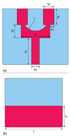
Figure 2 Reference antenna schematic: top view (a) and bottom view (b).
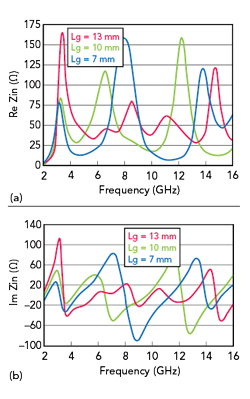
Figure 3 Input impedance as a function of lg: real (a) and imaginary (b).
Reference Antenna
The reference antenna layout is shown in Figure 2. The height of the ground is denoted as lg. The parameter lg represents the length of the microstrip feedline as well, which plays a key role in impedance matching to the 50 Ω SMA input connector (see Figure 3).