


Figure 1 Direct RF transceiver using direct conversion.
RF semiconductor and sampling technologies are advancing rapidly. Combinations of these technologies have yielded high speed RF analog-to-digital converters (ADCs) and digital-to-analog converters (DACs) capable of direct conversion between digital and Ka-Band, decreasing the need for analog RF front-ends (RFFEs) and simplifying transceiver systems.
Use of these new converters in semiconductor devices, such as digital RF transceivers and RF system-on-chip (RFSoC) devices, has enabled decreases in size, weight and power that were previously not achievable and flexible, on-chip digital up-conversion (DUC), digital down-conversion (DDC) and filtering. A block diagram for a digital RF transceiver using direct conversion is shown in Figure 1.
Digital RF transceivers and RFSoCs are being increasingly used in downstream devices, such as transmit/receive modules (TRMs), software-defined radios (SDRs) and commercial terrestrial and satellite communication (satcom). Since these devices now include mixed-signal RF and digital interfaces, traditional measurement approaches using vector network analyzers (VNAs) are no longer useful. A new approach for testing is needed.
AESA AND TRM BACKGROUND
The first phased arrays in the early 1900s were mechanically scanned using switches. Today’s active electronically scanned arrays (AESAs) use many solid-state TRMs or digital receiver exciters (DREXs), each connected to one or more antenna elements. Figure 2 shows an example of a new generation AESA with phased array antenna elements visible on the face of the antenna.
Architecting of the AESA with TRMs/DREXs was made possible by advancements in RF semiconductor technology in the 1980s. Today, even newer technologies and device types are available for high-power transmit amplification and low noise receive amplification. Leveraging these advancements, the size, weight, power and cost (SWaP-C) of TRMs/DREXs have been reduced, and usage is building in commercial applications such as satcom.
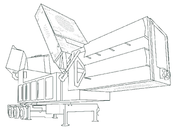
Figure 2 AESA antenna with visible TRM antennas.

Figure 3 Notional block diagram of an analog TRM.
TRMs and DREXs provide a range of functionality in an RF system, including high-power amplification (HPA) for the transmitter, low noise amplification (LNA) for the receiver, phase shifting to steer the AESA “beam,” and circulators and switches to route signals. Figure 3 shows a notional block diagram of an analog TRM.
Newer digital TRMs (DTRMs) transmit by receiving high speed serial (HSS) data from the RF system, applying serial to parallel conversion, converting to RF and amplifying to the required level using an HPA. Likewise, DTRMs receive by amplifying with an LNA, converting to digital, then applying parallel to HSS conversion. If the frequency is in the Ka-Band or below, this often leverages digital RF transceiver devices to handle RF to digital conversion as close to the antenna as possible, enabling additional signal processing functions in the DTRM, including DDC, DUC and filtering.
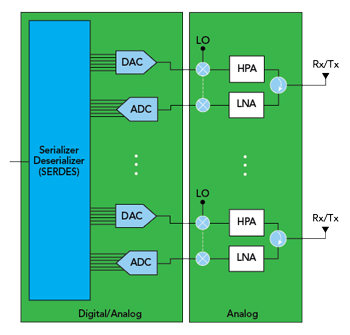
Figure 4 Block diagram of a multichannel DTRM.
DTRMs often use multichannel digital RF transceivers with 16 or higher channels on a single semiconductor device. Figure 4 shows a high-level block diagram of a multichannel DTRM with antennas.
AESAs configured with DTRMs offer additional advantages over analog TRMs, including increased flexibility and reduction in SWaP-C. However, the evolution to DTRMs also presents new challenges, including how to test multichannel DTRMs from “RF to Bits” in prototyping, development, characterization, hardware-in-the-loop (HIL) and production test phases.
WHAT IS REQUIRED TO TEST A TRM?
Analog TRMs have traditionally been tested using systems including VNAs, vector signal generators (VSGs) and vector signal analyzers (VSAs). Depending on the stage in the TRM test cycle, combinations of these instruments can be used to extract the desired measurement parameters.
Classical VNAs fundamentally provide small signal S-parameter measurements, such as gain, input match and output match, and enable calibration of the TRM using a range of transmit and receive gain and phase settings. In addition to CW measurements, some VNAs can also be useful for pulsed measurements, enabling measurement of semiconductor devices in the PA that are unable to operate at 100 percent duty cycle due to device heating.
The pairing of a VSG with a VSA (VST) provides additional measurement capability that is required for some stages of testing. These instruments enable the test engineer to excite the TRM with a modulated waveform and measure wideband signal parameters on the output. A range of potential measurements is enabled using these types of instruments, including noise figure (NF), adjacent channel power (ACP), error vector magnitude (EVM), third-order intercept (TOI/IP3), spurious free dynamic range (SFDR), power-added efficiency (PAE), large signal parameters and others.
Multichannel TRMs present special challenges, as channel-to-channel isolation and relative characteristics between channels may be required. Multiport VNAs can be used to measure isolation between channels, per-channel gain and phase response. However, CW stimulus and measurement techniques used with multiport VNAs are fundamentally different from real-world modulated signals. Multichannel VSTs can simultaneously stimulate and measure all ports of the multichannel TRM using wideband, phase-aligned signals, enabling measurements in a configuration matching usage conditions. An example of a 4-channel, phase-aligned VST is shown in Figure 5.
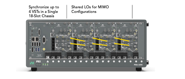
Figure 5 4-channel, phase-aligned VST.
As described in the previous section, DTRMs no longer have an analog input/output for testing, so these traditional instruments are of limited utility. New solutions matching the mixed-signal nature of DTRMs are required, with the capability to make new measurements that are analogous to VNAs, VSGs and VSAs.
SDR BACKGROUND
SDRs are a more recent development than TRMs, having been initiated in the 1980s and accelerated by recent developments in RFSoCs. SDRs consist of a few fundamental building blocks, which could either be monolithic or distributed, including RFFE and digital I/Q baseband (Direct RF conversion), stream signal processing and host controller. A block diagram for a generic SDR is shown in Figure 6.
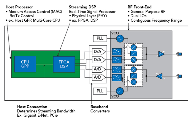
Figure 6 Generic SDR architecture.
Assuming that the board set for an SDR includes at least an integrated RFFE and digital I/Q baseband, DTRM and SDR test needs are very similar.