

EVOLVED MIXED-SIGNAL TEST SYSTEM
The major change in the transition from analog TRMs to DTRMs is the replacement of one of the RF ports with an HSS bus. Likewise, SDRs have a similar configuration with both HSS and RF interfaces. A new means of emulating HSS signals with the test system is needed to meet measurement needs for these new mixed-signal devices.
A complete single-box test system providing four channels of RF transmit (Tx) and receive (Rx) capability, as well as four channels of HSS Tx and Rx capability, is shown in Figure 7. Details of the test system components are provided in the following section.

Figure 7 Single-box, 4-channel RF and HSS test system.
Evolved Mixed-Signal Test System Components
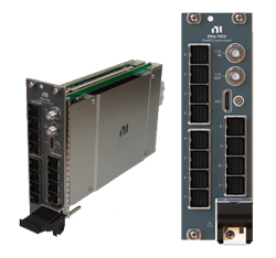
Figure 8 NI PXIe-7903 Flex-RIO HSS module. Source: Based on Xilinx Virtex UltraScale+ VU11P FPGA with 48 multi-gigabit transceivers.
Emulation of transmission and reception of HSS signals can be achieved using various approaches, most of them based on user-programmable FPGAs. Development boards from FPGA manufacturers are one option, but they can have short support lives and lack the ability to be synchronized with the test system. A modular commercial off-the-shelf (COTS) solution would be a superior solution, providing a user-programmable FPGA and flexible electrical or optical HSS interface as well as synchronization with the test system through the PXI backplane. An example of this solution is shown in Figure 8.
HSS formats used for DTRMs and SDRs are not standardized, and can include various formats such as JESD-204C, 100 GbE, Vita 17.3 and Aurora. Each of these formats has user-selectable options, including the number of lanes, encoding and bit depth. Based on the multitude of HSS formats and the potential range of user-selected options for each format, semi-custom IP is typically needed for the FPGA, matching the implementation for the device(s) to be tested.
Modulated RF signal generation and analysis, and matching the frequency range and bandwidth to be tested, are needed on the RF side of the device under test (DUT). Depending on the DUT configuration, either a single-channel or multichannel solution could be required. If the DUT is multichannel and simultaneous measurement capability is needed, a multichannel VST solution is necessary. However, if sequential measurements are acceptable, a single-channel VST with RF switching could be used. In either case, synchronization with the FPGA-based HSS solution is required. A modular VST solution is shown in Figure 9, enabling synchronization with the test system through the PXI backplane, similar to the COTS FPGA solution.

Figure 9 NI PXIe-5842 VST module.
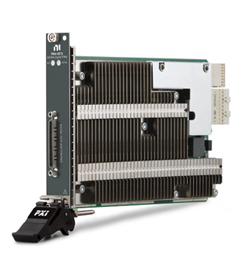
Figure 10 NI PXIe-6571 digital pattern instrument.
In addition to HSS and RF I/O, DTRMs and SDRs typically require state control signals. These are usually provided over SPI, I2C, MIPI or other interfaces. Ideally, these control signals would be synchronized with the test system so that the timing of HSS and RF could be tightly controlled.1 A multichannel, SW-configurable solution to provide a large array of control signals is shown in Figure 10. This includes synchronization with the test system through the PXI backplane, as in other examples.
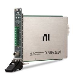
Figure 11 NI PXIe-4139 source measure unit.
Lastly, the DTRM or SDR needs power from the test system. In cases where high-power PAs utilizing GaN technology are used, power must be pulsed and measurements must be made during the “on” cycle of the device. In addition, DTRMs or SDRs may require multiple voltage rails with specific turn-on/off sequences. A power supply (source measure unit) capable of providing continuous or pulsed power in synchronization with the test system is shown in Figure 11.
MIXED-SIGNAL MEASUREMENTS FOR DTRMS AND SDRS
While traditional VNA RF in/RF out measurements are no longer applicable for DTRMs and SDRs, analogous single or multichannel measurements with HSS in/RF out and RF in/HSS out are now possible, leveraging the system and components described in the previous sections.
Traditional VST-based Tx measurements can be emulated using a combination of HSS bit stream(s) into the SDR or DTRM, and measurement of RF output(s) from the device. Measurements on the resulting RF signal can be made, including generic time-domain and frequency-domain measurements as well as standards-based measurements like ACP and EVM. Two-tone measurements like TOI can be emulated using dual tones encoded in the HSS stream. PAE can be measured for various types of input signals by measuring RF output power and input DC power and calculating the ratio of the two.
Likewise, analogous measurements to traditional Rx measurements, such as BER/BLER, can be constructed using modulated RF signals into the SDR or DTRM, and demodulated digital I/Q from the HSS stream. NF measurements can be measured using traditional Y-Factor techniques and monitoring the amplitude of the HSS digital I/Q stream.
Mixed-signal analogs to traditional VNA S-parameter measurements are challenging to construct, but some pre-work has been done in academia.2 Standard VNA measurements use ratios of forward and reverse signals (A-incident and B-reflected waves) measured at calibrated reference planes. It is difficult to implement a similar approach with mixed-signal devices due to challenges, including a lack of a reference plane and suitable calibration standards on the digital side. Work continues to identify a suitable set of approaches.
CONCLUSION
DTRMs and SDRs require test solutions tailored for mixed-signal devices in development to production test stages. While measurements between these phases are similar, different phases have different requirements, such as accuracy, speed and other factors.
Test solutions for legacy analog TRMs have consisted of VNAs, VSGs and VSAs, but newer DTRMs require evolved capability to make mixed-signal measurements with HSS data streams and RF signals. Measurement requirements for SDRs require a similar mix of HSS and RF.
A solution has been proposed leveraging FPGA-based HSS, VST-based RF, power supply and control, all synchronized using PXI-based timing and synchronization with sub-nanosecond accuracy. This solution offers benefits including accuracy of traditional VSG and analysis, customized FPGA-based HSS interface matching the DUT configuration and the ability to leverage PXI-based timing and synchronization to provide fast changes in power, control, HSS and RF configuration to accelerate measurements of mixed-domain devices.
References
- NI PXI Timing and Synchronization Design Advantages, NI.
- D. C. Ribeiro, A. Prata, P. Miguel Cruz and N. Borges Carvalho, “D-Parameters: A Novel Framework for Characterization and Behavioral Modeling of Mixed-Signal Systems,” IEEE Transactions on Microwave Theory and Techniques, Vol. 63, No. 10, October 2015, pp. 3277–3287.
- F. Verbeyst, P. Barmuta, M. Vanden Bossche and M. Rullmann, “Accurately Applying Wideband Modulated Signals to a DUT Using an Extended VSG-VSA Setup” ARFTG, June 2, 2023.