
In this article, a new pulsed I/V measurement technique for observing the dependence of the IV characteristics of a MESFET device on frequency, electric field and self-heating effects is presented. The results obtained with the new procedure are compared with experimental data obtained with conventional pulsed and static IV characterization systems. The new experimental approach provides a better indication of the effect of these variables on the IV characteristics of the MESFET device and is particularly useful in nonlinear switching applications. The experimental work considers how the dependency of the drain current on frequency and electric field can be incorporated, in an implicit manner, in the mobility figure for the device. The measurement procedures considered here can also be usefully applied to the HEMT device where the frequency dispersion, electric field and thermal effects are just as significant.

Measurements and Devices
The measurement system employed to investigate the frequency, electric field and temperature dependency of GaAs devices is shown in Figure 1.1 The static and pulse power supplies associated with the gate-source and drain-source junctions are identical and independent. Through program control, a wide range of different measurements can be carried out. For the purposes of this paper, the most relevant are as follows:
Static IV measurements:
These can be performed using different sweep rates to enable the extent of the self-heating effect to be observed. For the results presented in this article, a one second delay was used at each bias point, prior to measuring the drain current. This time is sufficiently long for the device to reach equilibrium conditions from a thermal point of view.2
Pulsed IV measurements:
These can be performed by pulsing the gate-source and drain-source terminals together, or independently from different static points. For the case where only the gate-source terminal is pulsed, the drain-source terminal is swept in a normal DC manner. For the case where only the drain-source terminal is pulsed, the gate-source junction is swept in a normal DC manner. For the case where both junctions are pulsed, the width of the drain-source pulse is smaller than the width the gate-source pulse. The latter is applied first to ensure that the initial current through the device is well controlled. From a frequency point of view these three measurements are the same. This is also true from a power dissipation and thermal point of view since the drain-source resistance of the device is high when it is biased in the off condition (> 30 kΩ). Since the pulse employed were 1 µs wide (with a rise and fall time of 50 ns) and a period of 1 ms, no self-heating effect from the dynamic bias conditions is introduced into the device.2-5 Self-heating effects are, therefore, determined by the static conditions employed for the pulse measurements. In this article, all the pulsed results presented were obtained from the static point of VGS static = -1 V, VDS static = 0 V where the device is off and there is no self-heating from the static bias. This condition was applied to ensure that only the effects of the biasing conditions are observed. The drain current value obtained from this measurement is the average of 16 readings, which are taken once the pulse has settled.
Pseudo-random pulsed IV measurements:
This is a novel pulse IV measurement idea that enables the true extent of the dependency of the device IV characteristics on the above variables to be observed. A clearer understanding of the method used to implement this measurement can be obtained by considering a specific case.
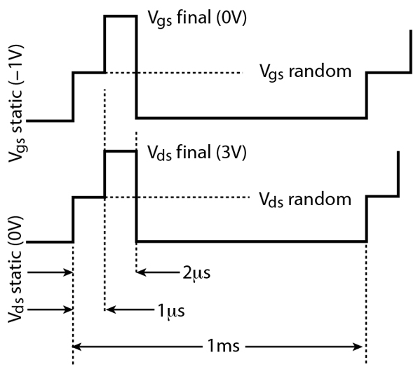
If it is assumed that the static supplies are set to VDS static = 0 V and VGS static = -1 V (the device in the off condition and therefore no self-heating effects) and the drain current at the dynamic bias point of Vds dynamic = 3 V, Vgs dynamic = 0 V is to be measured, then the two-step process shown in Figure 2 is employed. The amplitude of the dynamic pulses denoted as Vds random and Vgs random is determined using a pseudo-random algorithm.
The maximum and minimum values of these pulses are constrained by the user to fall within a specified dynamic bias range. For this case, this could be in the 0 to 4 V range for the drain-source junction and -1 to 0 V for the gate-source junction. The base potential of these pulses is clearly the VDS static = 0 V, VGS static = -1 V static point. After 1 µs a further pulse is launched, whose base potential is the dynamic pseudo-random value and the final potential is the dynamic destination value.
Once the value of the drain current is noted, the pulse amplitude returns to the static conditions and remains there for 1 ms to ensure that no self-heating takes place. The drain current at the same dynamic point is then measured again, using different pseudo-random values. If this process is repeated a large number of times, then an appreciation of the dependency of the IV characteristics on electric field changes can be obtained. For the results presented here, each dynamic bias point was measured in this way using 1000 samples. This provides a reasonable statistical distribution and, because of the speed by which this measurement system performs this task, it is an operation that can be performed quickly. In some respects, this measurement idea is similar to the eye diagram measurements commonly performed by the communications industry. In this case, however, it is the base line of the pulse that is varied rather than the pulse width.
It is worth noting that the polarity of the pulses employed for these measurements can be positive, negative or zero. This depends on the value of the static bias point, the value of the pseudo-random bias and the final or dynamic bias value to be measured.
In the previous discussions, the pulsed measurements have employed a pulse width and period corresponding to a measurement frequency of 1 kHz. This condition is commonly used on the grounds that the characteristics of the device remain reasonably constant beyond 1 kHz and the self-heating effect is small. This assumption, however, needs to be reconsidered because of the inter-dependency between the electric field conditions and frequency. If such a dependence is to be assessed, it is necessary to repeat the above measurements with different pulse widths and periods so that the effect of frequency on electric field can be characterized. Results for such measurements will be presented later in the article.
To demonstrate the measurement method, a 4-finger, 225 µm gate-width MESFET device from GEC Marconi Materials Research Ltd. was used. Similar results have been observed with other devices. The device is an ion-implanted, gate recessed MESFET with a 0.5 µm gate-length and a pinch-off voltage of -0.8 V.
Experimental Results
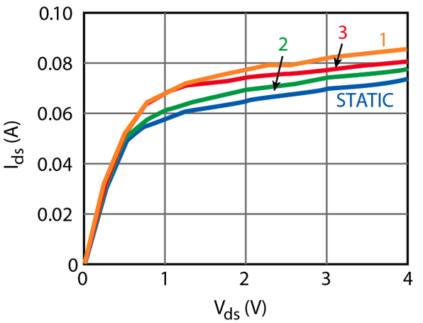
Figure 3 shows a number of curves measured under static and pulsed conditions using pulse widths of 1 µs with a period of 1 ms. The curve for the static case corresponds to VGS static = 0 V, and was measured with a one second delay time between points to ensure that the self-heating effect reaches equilibrium conditions. The remaining curves were measured under different pulsed conditions. For all these pulsed cases, the end or dynamic value of VGS dynamic corresponds to 0 V so that the pulsed curves can be compared with the static curve.
Curve 1 corresponds to the case where only the drain terminal is pulsed from the static point of VDS static = 0 V. For this case the gate terminal is not pulsed and is fixed at VGS static = 0 V. The difference between curve 1 and the static curve is, therefore, due to frequency, electric field and temperature effects. For the static curve, the drain-source resistance of the device is 230 Ω. This reduces to 192 Ω when the device drain terminal is pulsed.
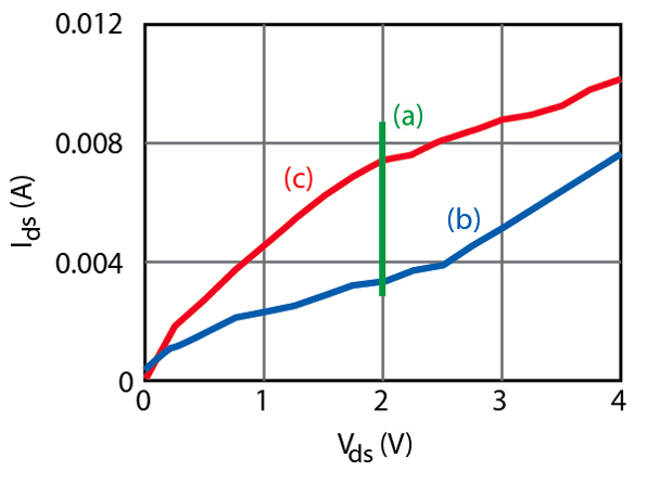
Curve 2 corresponds to the case where only the gate terminal is pulsed from the static point of VGS static = -1 V where the device is firmly pinched-off. The drain terminal is not pulsed but is merely swept in a normal DC manner. If electric field effects were not an issue, then curve 1 and curve 2 should coincide, since in both cases the measurement frequency, the power dissipated and the ambient temperature of the device is the same. The difference between curve 2 and the static curve is due to electric field, frequency and temperature effects. As was demonstrated in an earlier article,6 however, the self-heating effect is small compared with the other variables. For curve 2 the drain-source resistance is 216 Ω , which is closer to the DC value than when the drain terminal is pulsed.
The final interesting case to consider is curve 3, which corresponds to the situation where both the gate and drain terminals are pulsed from the static point of VGS static = -1 V and VDS static = 0 V. From a measurement frequency, power dissipation and temperature point of view, this situation is the same as curve 1 and curve 2. The results, however, differ considerably from the two earlier pulsed cases. This illustrates quite clearly the dependence of the characteristics of the device on the electric field conditions that is different for the three cases considered.
The large dependency of the IV characteristics of the device on the electric field conditions brings into question whether the results provided by conventional pulsed IV measurements such as those described above and elsewhere5-8 should be viewed as a straightforward thermal effect.
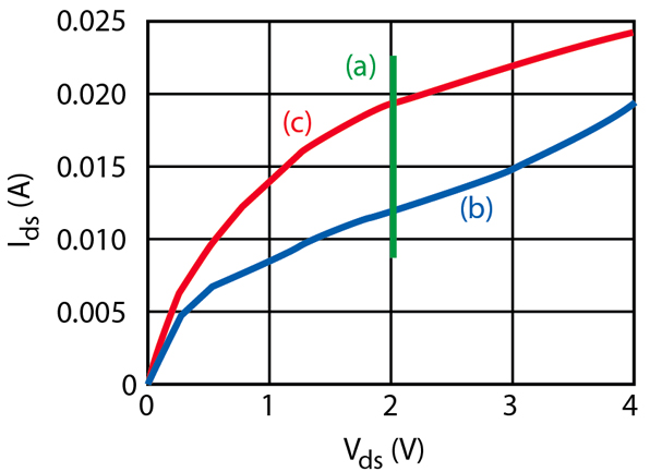
To illustrate the problem more clearly, in Figure 4, the drain currents of the device are compared when measured with the pseudo-random method (at the VGS dynamic = -0.4 V, VDS dynamic = 2 V point), the normal DC method and the normal pulsed method (the gate and drain pulsed) for the Vgs static/dynamic = -0.4 V curve. At this gate-bias the dynamic power dissipation is lower than for the previous test. For the normal pulsed method, the static bias point corresponds to VDS static = 0 V, VGS static = -1 V. For the normal DC method, a one second settling time was used. The pseudo-random data presented here re-enforces the point that the differences between the pulsed curve and the static curve are not due to the self-heating effect alone but also to the frequency and electric field effects. The most important feature to note, however, is that the conventional pulsed measurement approach provides data that is specific to the conditions in use. Such an approach does not provide suitable feedback on how the characteristics of the device are altered when the electric field conditions are altered in an unpredictable manner as is required for the development of a general-purpose model. Notice, for example, that the pseudo-random data produces excursions on the drain current that fall outside of the range of values provided by the conventional measurements. For the pseudo-random case, the measurements were performed using positive and negative going pulses since the dynamic bias point under consideration is approximately half way along the VDS dynamic and VGS dynamic bias plane.
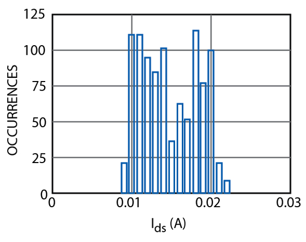
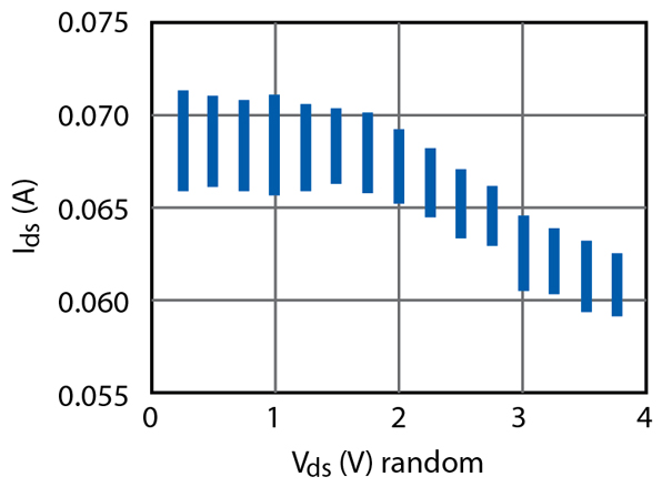
The statistical distribution of the measured drain current at this point is shown in Figure 5. A similar distribution was found for the other bias points considered. For these other bias points, however, the valley or minima on the center of the histogram varied according to the value of the bias point being measured. This valley depends on the bias point to be measured, the pseudo-random value and whether a positive or negative going pulse is used.
A similar picture emerges when a lower drain current area is considered, as is shown in Figure 6 for the Vgs static/dynamic = -0.6 V case. This data re-enforces the view that this variation in the drain current is not due to self-heating effects arising from the dynamic bias conditions employed. Notice, for example, that the dynamic power dissipated in the device in this test is much lower than in the earlier tests, but the variation in the drain current is just as significant.
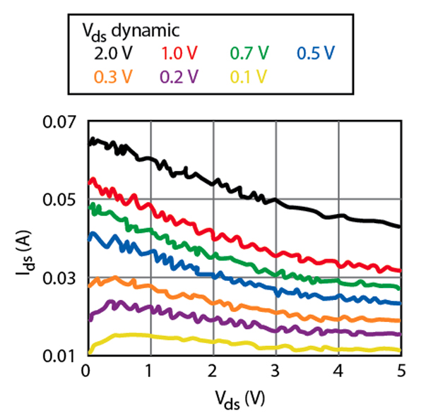
In Figure 7, the measured drain current of the device is shown at Vds dynamic = 4 V, Vgs dynamic = 0 V point as a function of the pseudo-random drain-source and gate-source voltage. This data was measured from the static bias point of VDS static = 0 V VGS static = -1 V and represents 1000 samples. Since the pseudo-random bias voltages for the gate-source and drain-source junctions were constrained as stated earlier, and because of the final destination value selected, the pulses generated in these measurements were all positive going. The large change in the drain current as the electric field is varied on either the gate-source or drain-source junctions is quite interesting. From these results, it is seen that the dependency of the current per unit change in electric field is the same for the gate-source and gate-drain junctions. It should be remembered that this variation in the drain current arises from an event which took place 1 ms earlier. It should also be remembered that, because the variation of the pseudo-random bias to the device is random, the x-axis (and z-axis) data should not be considered in the usual time-dependent manner. The drain current corresponding to the Vds random = 4 V point, for example, could have been measured first rather than last as with a conventional system. The low pass filter type of characteristics as the drain-source junction potential changes is also worthy of note.
This effect is not, of course, restricted to the saturation region. In Figure 8, for example, the drain current is compared as a function of the pseudo-random drain-source dynamic voltage for different drain-source dynamic destination values at Vgs dynamic = 0 V. As can be seen in the linear region, the dependency of the traps on electric field is just as relevant as in the saturation region.
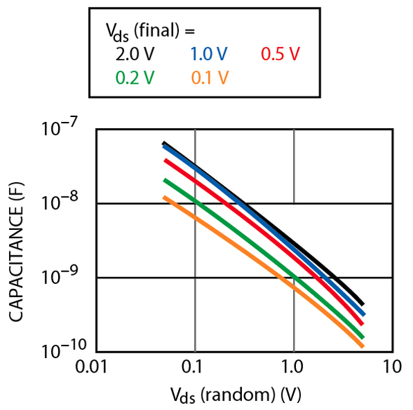
This data can be represented as a capacitance-voltage graph, as shown in Figure 9, using a log scale for the x- and y-axis. These results were computed using the familiar expression

A time of 50 ns, which corresponds to the rise and fall time of the pulses employed, was used in the above calculations. This capacitance data corresponds to a measurement frequency of 1 kHz. The results show that the variation of this low frequency capacitance with electric field follows the classic depletion capacitance form.
A more useful form of representing the data is to estimate the mobility figure for the device. This can be done as a function of static or dynamic bias and, if the measurements are repeated at different frequencies, the effect of frequency on the mobility value can be established. The calculation of the mobility figure, at any bias and frequency point, employed the approximate small-signal linear expression for mobility9

where
Cg = gate capacitance
gm = device transconductance
vds = voltage applied to the drain terminal
Rs = source resistance
Rd = drain resistance
Rds = drain-source resistance
L = gate-length of device
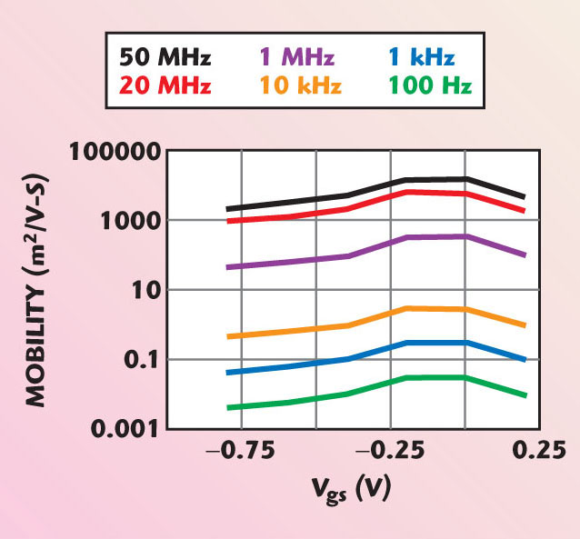
In the application of this equation, the value of gm and Rds were estimated by differentiating the dynamic values of Ids with respect to Vgs dynamic and Vds dynamic, respectively. The parasitic resistances Rs and Rd were determined from S-parameter measurements. In this work, the frequency range of interest is quite low (100 Hz to several kHz) since the frequency area of interest is where the device IV characteristics are known to be strongly frequency dependent. The dependency of the electron mobility on these variables for the device above is shown in Figure 10 as a function of Vgs for several frequencies. The strong nonlinear dependency of mobility on the gate-source bias is clearly evident and not unexpected. The very strong dependency of the mobility on frequency is also not unexpected since the majority of the device model parameters are known to be frequency dependent. This is especially true of gm and Rds, which are strongly frequency dependent. The frequency dependency of these parameters is, of course, implicitly included in the mobility value obtained. When considering the mobility results, it should be remembered that the measurements performed are large-signal nonlinear measurements, whereas the equation for mobility was originally developed for a device operating in the linear region under small-signal conditions. It is for this reason that only the results for low values of Vds dynamic have been considered in this graph. Mobility results for the device operating in the linear and saturation regions will be presented in a later article.
The representation of the data in the form shown above is, from a modeling point of view, more satisfactory than the capacitance format. This is because the dependency of the IV characteristics on frequency and electric field changes can be incorporated in most drain current expressions with relative ease. This issue is under consideration at the moment and results will be published at a later date.
Conclusion
A new experimental system for observing the dependence of the IV characteristics in GaAs devices on electric field and frequency has been presented and compared with conventional measurements. The results indicate a much larger dependence in the device IV characteristics due to electric field and low frequency changes than previously thought. This behavior is true in the saturation and linear regions of operation under low and high current modes of operation. The dependencies of the IV characteristics on electric field and frequency can be included in the mobility figure for the device. As far as it is known, mobility results under large-signal conditions have not been presented previously.
References
1. T. Fernandez, Y. Newport, J. M. Zamarillo, A. Mediavilla and A. Tazon, "High Speed Automated Pulsed IV Measurement System," 23rd European Microwave Conference, Madrid, Spain, September 1993, pp. 494-496.
2. J. Rodriguez-Tellez, A. Mediavilla, T. Fernandez and A. Tazon, "A Method for Characterising Frequency Dispersion and Thermal Effects Independently in GaAs FETs," European Microwave Conference, Munich, Germany, October 1999, pp. 399-402.
3. J. Rodriguez-Tellez, N.T. Ali, T. Fernandez, A. Mediavilla and A. Tazon, "Electric Field Dependency of Traps in MESFET/HEMT Devices," European Microwave Conference, London, England, September 2001, pp. 24-25.
4. J.M. Golio, M.G. Miller, G.N. Maracas and D.A. Johnson, "Frequency Dependent Electrical Characteristics of GaAs MESFETs," IEEE Transactions on Electron Devices, Vol. 37, May 1990, pp. 1217-1227.
5. J.A. Higgings, "Thermal Properties of Power HBTs," IEEE Transactions on Electron Devices, Vol. 40, December 1993, pp. 2171-2177.
6. J. Rodriguez-Tellez, T. Fernandez, A. Mediavilla and A. Tazon, "Characterisation of Thermal and Frequency Dispersion Effects in GaAs MESFET Devices," IEEE Transactions on Microwave Theory and Techniques, Vol. 49, No. 7, July 2001, pp. 1352-1355.
7. J.P. Teyssier, P. Bouysse, Z. Ovarch, D. Baratand, T. Peyretaillade and R. Quere, "40 GHz/150ns Versatile Pulsed Measurement System for Microwave Transistor Isothermal Characterisation," IEEE Transactions on Microwave Theory and Techniques, Vol. 46, No. 12, December 1998, pp. 2043-2052.
8. A.E. Parker and J.B. Scott, "Method for Determining Correct Timing for Pulsed I/V Measurement of GaAs FETs," IEE Electronic Letters, Vol. 31, September 1995, pp. 1697-1698.
9. R.A. Pucel and C.F. Krumm, "Simple Method of Measuring Drift Mobility Profiles in Thin Semiconductor Films," Electronics Letters, May 1975, Vol. 12, No. 10.