
SMA, 3.5 mm and 2.92 mm connectors make reliable, RF components and instrumentation possible. These seemingly mundane devices are the result of evolutionary and revolutionary design, covering a 40-year period and involving several corporations. In their present state, they represent highly evolved, well-defined interface systems. It is not widely understood that these connector types are mechanically intermateable; meaning, SMA, 3.5 mm and 2.92 mm connectors, of good quality and in good condition, will inter-mate across connector families without damage.
But what are the electrical ramifications of inter-mating of these connector types? Can they be used interchangeably without an appreciable difference in performance, that is, will a significant impedance discontinuity occur when mixing types? Were they intended to be inter-mated in the first place? To properly answer these questions calls for a brief examination of the history and motivations behind these connectors.
The SMA Connector
The SMA connector first appeared in the late ’50s as the “BRM,” manufactured by the Bendix Scintilla Division. In the ’60s it was popularized as the “OSM,” manufactured by Omni Spectra. In 1968 it received the “SMA” (Sub-miniature A) designation that we know today.
The SMA connector uses a solid dielectric interface as opposed to an air dielectric. By definition, an air interface connector cannot have the designation “SMA.” Performance is rated to 18 GHz, but higher frequency variants are available.
The SMA was designed as a miniaturized, economical connector for system application. It was never intended to be a precision connector for the laboratory. As it is only rated for 500 mate/de-mate operations, it was designed for use in semi-rigid cable assemblies and components not requiring frequent connect/ disconnect.
The 3.5 mm Connector
The 3.5 mm connector was the result of a joint venture in the early ’70s between Hewlett Packard (now Aglient Technologies) and Amphenol. Hewlett Packard carried out the bulk of the development work and Amphenol manufactured the connector, dubbing it the “APC3.5” (Amphenol Precision Connector 3.5 mm). Hewlett Packard’s design goals included the following:
• a durable interface that would extend the upper frequency capability of their devices to 26.5 GHz
• an interface allowing for thousands of repeatable connections, and one that would mate with popular SMA dimensions
The 3.5 mm connector is rated to 26.5 GHz, with a theoretical upper operating frequency of 34 GHz. It is specified to possess a minimum of 3000 mate/de-mate cycles per the IEEE P287/D3 standard (provisional). The 3.5 mm connector was designed to be a precision interface for calibrated measurements of SMA-equipped devices—it was created as a test connector for the SMA. As a result, an SMA-to-3.5 mm interface produces better results electrically than an SMA-to-SMA interface.
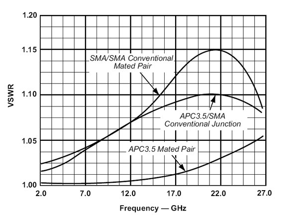
The reason is due to an air gap that is formed between the solid dielectric interfaces of a mated pair of SMA connectors, creating an impedance discontinuity (see Figure 1).
With this information, it can be seen that an SMA-to-3.5 mm mated interface, using good quality connectors, is an acceptable (and intended) practice where adverse electrical performance through 18 GHz should not be expected.
The 2.92 mm Connector
The 2.92 mm geometry with an SMA mateable interface was developed to provide coaxial connector performance to 40 GHz. In the mid-’70s, Maury Microwave introduced the MPC3 connector using the aforementioned 2.92 mm geometry. Without an abundance of available instrumentation operating at 40 GHz, it found little usage. In the early 1980s, Weinschel Engineering utilized this geometry in an engineering design under a Department of Defense (DoD) contract.
Simultaneously, Wiltron Co. began a program to produce instrumentation operating to 40 GHz, and would therefore use the 2.92 mm connector. The connector and instrumentation were introduced in 1983 by Wiltron (now Anritsu Corp.); the term “K-connector” was trademarked by Wiltron, making reference to the connector’s frequency band of operation, the K-band. Intermateability with the SMA was not an original design objective for the 2.92 mm connector.
The ability of these two connector types to inter-mate grew out of convenience; the 2.92 mm was based upon proven SMA geometry.
Basic Assumptions Established
Now that the basic relationship between these three connector types has been explained, characterizing the electrical performance of these connector types when inter-mated can be addressed. It has been established that a 3.5 mm-to-SMA mated interface is an acceptable and intended practice, per the 3.5 mm connector design. All that remains is to demonstrate the electrical performance of a 3.5 mm-to-2.92 mm mated interface and a 2.92 mm-to-SMA interface.
A Few Words Regarding Wear
The premise of intermateability is predicated upon connectors that are in serviceable condition. Misaligned center contacts or contact heights out-of-spec, worn outer conductors—especially in SMA designs—invite damage and a reduction in performance. Mating interfaces must be inspected and cleaned regularly. Pin height gauges are not reserved for metrology-grade applications; they are a good idea for anyone working with these connector types in frequent mate/de-mate scenarios.
Electrical Performance at the Connector Interface
Across the SMA, 3.5 mm and 2.92 mm connector types, a governing factor in electrical and mechanical performance is center contact height—a measure of protrusion or recession of the center contact with respect to the connector reference plane.
Depending upon whether the connector is a LPC (Laboratory Precision Connector)-based or GPC (General Precision Connector)-based design, the center contact height has a prescribed allowable range; temperature and wear can impact variation within this range. Center contact height is a compromise between good mechanical performance, that is, non-destructive contact with its mating connector, and good electrical performance. But how does center contact height influence electrical performance?
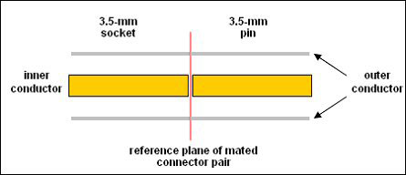
A mated pair of 3.5 mm connectors is shown in Figure 2 under ideal center contact height conditions. In other words, there is minimal gap or “zero gap” between the pin and socket center contact sections at the reference plane. Gap length is a direct result of contact height. This arrangement is considered ideal as it produces the smoothest impedance transition through the mated pair. However, it will not tolerate use over a range of temperatures; expansion at high temperatures may cause destructive mating to occur.
Figure 3 shows the same mated connector pair with the 3.5 mm pin in a recessed condition. In this exaggerated example, a gap is produced at the reference plane resulting in an inductive or high impedance section. The gap provides the necessary clearance for over-temperature use, but also introduces an impedance discontinuity.

Although there are other areas of potential variation, connector center contact height variation plays a major role in defining interface electrical and mechanical performance. Good-quality 3.5 mm, 2.92 mm and SMA connectors—those whose interfaces are produced in accordance to the IEEE 287 (3.5 mm and 2.92 mm) and MIL-STD-348 (SMA) specifications—will have their critical dimensions constrained.
These specifications/standards serve to support the practice of intermating these connector types. It is important to note that the IEEE 287 and MIL-STD-348 specifications address interface dimensions only; they do not touch upon design issues associated with a connector’s “back end” or cable interface side. This issue is to be resolved by the manufacturer.
Performance Questions Answered
An experiment was devised to investigate the impact of center contact height (mated contact gap) variability on interface electrical performance within mixed mated pairs of connector types (3.5 mm-to-2.92 mm and 2.92 mm-to-SMA, for example).
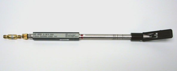
To establish a reference, electrical performance vs. center contact height was examined using a mated pair of 3.5 mm connectors. Single-port VNA measurements through 26.5 GHz were made with LPC grade 3.5 mm connector adapters coupled to a 3.5 mm sliding load from an HP85052B 3.5 mm calibration kit. The adapter/ sliding load arrangement is shown in Figure 4.
A sliding load was selected for two reasons: (1) it contains a sufficiently long 50 &Omega air line section that will facilitate gate placement for time domain gating operations used in the data analysis portion of the experiment; (2) the center contact height of the sliding load 3.5 mm interface is variable via an adjustment screw located at the rear of the sliding load. This allows for precise control of the gap between the 3.5 mm socket and 3.5 mm pin contacts when mated.
The experiment consists of the following steps:
• Using the mated pair of 3.5 mm connectors as an example, one end of the 3.5 mm LPC grade socket adapter was threaded into port 1 of the VNA
• Using a center contact height gauge, commonly called a pin height gauge, the sliding load interface-pin type was gauged and center contact height was adjusted to 0.0000 inches.
• The sliding load was then threaded onto the LPC 3.5 mm socket interface and tightened to the appropriate torque specification. The result is a 3.5 mm socket-to-pin mated interface
• An S-parameter measurement was made of the 3.5 mm mated interface; the resulting S11 data was recorded for subsequent examination of the mated interface’s VSWR and impedance. The sliding load was removed from the 3.5 mm socket interface and contact height was lowered by 0.001 inches, as measured with the contact height gauge
• Repeat Steps 3 and 4 up to a contact height of –0.005 inches; the negative sign indicates a recessed condition, i.e., a position below the connector reference plane

The above steps were repeated using a 2.92 mm-to-3.5 mm mated interface and an SMA-to-2.92 mm mated interface. In these instances, a sliding load equipped with a 2.92 mm pin type interface was used in place of the 3.5 mm sliding load. Table 1 provides contact and dielectric height data (if applicable) for each mating socket interface type used in the experiment.
Performance Questions Answered: Summary of Findings
A rise in impedance occurs when terminating the mated interface pairs with a sliding load. This rise is due to a limitation inherent to the sliding load—the load’s “cut-off frequency.” The sliding load depicted in Figure 4 is recommended for use between 2.5 and 26.5 GHz. Below 1.8 GHz, the load displays an impedance of less than 50 Ω.
At very low frequency, near DC, the sliding load is a short. This irregularity causes reflected impedance measurements to rise with time, and the VSWR to tend towards a value slightly above 1.00:1 as the frequency tends to zero (see Appendix A).
With this in mind, the impedance and VSWR data are accurate in that they faithfully portray the behavior of a mated pair interface under the noted load conditions.
VSWR: In all three mated interface combinations (3.5 mm-to-3.5 mm, 2.92 mm-to-3.5 mm and SMA-to-2.92 mm), the VSWR never exceeded 1.054:1 through 26.5 GHz, over the range of experimental center contact gaps. The 3.5 mm and 2.92 mm-to-3.5 mm mated interfaces produced very similar VSWR results over the range of gaps, having a nearly identical spread in maximum VSWR values: 1.005:1 to 1.050:1 through 26.5 GHz. The SMA-to-2.92 mm mated interface produced a much tighter, but overall higher spread of maximum values: 1.038:1 to 1.054:1 through 26.5 GHz.
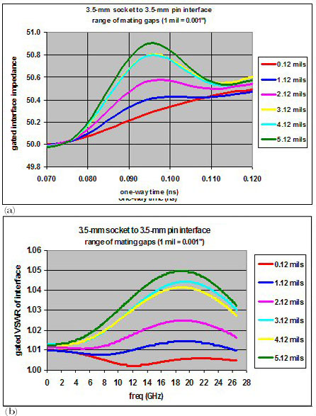
Impedance: Impedance was examined via a time domain step response. As expected, the mated interface impedance closely mirrored VSWR on all mated pair combinations. Out of the mated pair combinations tested, the 3.5 mm mated interface produced the most ideal response, having a nearly flat transition occurring at a contact gap of 0.12 mils (0.00012").
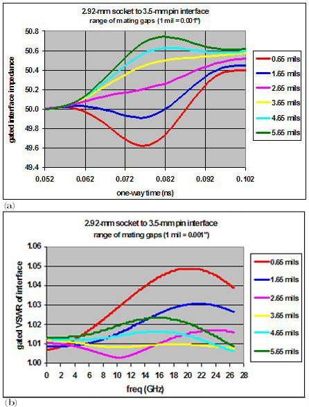
A close second in terms of ideal response was the 2.92 mm-to-3.5 mm mated interface, producing a similarly flat transition at a contact gap of 2.65 mils (0.00265"). In third place was the SMA-to-2.92 mm mated pair, providing its best impedance transition performance at a 1.50 mil (0.0015”) contact gap. Additional details on the data collection and analysis appear in Appendix A.
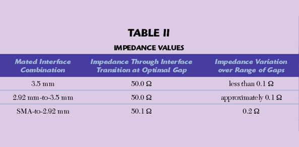
In Table 2, the impedance values are corrected to 50 &Omega to offset the previously mentioned rise in impedance. The table summarizes performance when the termination consists of a broadband 50 W load as opposed to a sliding load.
Conclusion
The experiment’s purpose was to investigate the influence of center contact gap variations upon a mated pair’s electrical performance; specifically, high frequency electrical performance. Gap variability was accomplished by varying the center contact height of one connector within the mated pair.
By systematically changing the gap, real-life mated connector pair performance across mixed interface types was modeled. Although differences in performance were noted, no significant advantages or disadvantages in electrical performance were observed across the mixed interface mated pairs. In short, the inter-mixing of 3.5 mm, 2.92 mm and SMA interface types was not found to produce adverse performance and significantly different results when using connectors made by a reputable manufacturer.
The 3.5 mm and 2.92 mm-to-3.5 mm mated interfaces produced somewhat better results compared to the SMA-to-2.92 mm mated interface. However, these results are the product of tightly controlled contact heights; center contact heights on the order of -0.00012" are not the norm and are associated with costly, special purpose LPC connector types.
The majority of applications employing 3.5 and 2.92 mm connectors utilize “test grade” versions of these connector types, that is, a grade of connector where center contact height is held at lower levels to accommodate frequent handling and use over temperature, thus wider mated center contact gaps will be encountered.
Test grade connectors can be made to comply with many of the IEEE 287 standards, but in specific areas, designers may choose to depart from these criteria for the sake of ease of manufacturing and/or cost concerns. In the end, the performance differences between these interface combinations are indeed very small even under controlled conditions.
Under non-controlled conditions, such as those that prevail in all but the most demanding metrology applications, these differences become insignificant.
Acknowledgments
The author extends his thanks to the following individuals without whose help this technical note would not have been possible: Harmon Banning, technologist, W.L. Gore & Associates Inc., Thomas Clupper, senior electrical engineer, W.L. Gore & Associates Inc., Jon Hvitfelt, RF connector designer, W.L. Gore & Associates Inc. and Marc Maury, president, Maury Microwave Corp.
References
1. Institute of Electrical and Electronic Engineers Inc., IEEE P287/D3 – Provisional, Standard for Precision Coaxial Connectors (DC to 110 GHz), July 2005.,/P>
2. Maury Microwave Corp., Application Note 5A-011, Improving SMA Tests with APC3.5 Hardware, November 18, 1999.,/P>
3. Maury Microwave Corp., Application Note 5A-021, Microwave Coaxial Connector Technology: A Continuing Evolution, December 13, 2005.,/P>
4. Agilent Technologies Inc., Application Note, General RF Connector Information, December 2000.,/P>
5. Department of Defense, United States of America, Interface Standard for Radio Frequency Connector Interfaces, MIL-STD-348A, April 20, 1988.,/P>
6. Department of Defense, United States of America, Performance Specification: General Specification for Connectors, Coaxial, Radio Frequency MIL-PRF-39012E, April 27, 2005.,/P>
Paul Pino received his BS degree in electrical engineering from the University of Delaware in 2000 after leaving a long career in the automotive industry. He joined W.L. Gore & Associates Inc. in 1999 and has worked with various groups including Gore’s Signal Integrity Lab, the Planar Cable Team, the Fiber Optic Transceiver Team and for the past four years the ATE Microwave Group.
Appendix A
Detailed Analysis of Experiment
Test Equipment Information
• Network Analyzer: Hewlett Packard 8510, equipped with 8517 test set equipped with 2.4 mm pin port connections; operational frequency range: 0.045 to 50 GHz
• Calibration Kits: For 3.5 mm and 3.5-to-2.92 mm mated interfaces, Hewlett Packard, Model 85038 3.5 mm calibration kit. For the SMA-to-2.92 mm mated interface, Maury Microwave, Model 2.92 mm calibration kit. Contact height gauges from the Hewlett Packard kit were used to gauge 3.5 and 2.92 mm interfaces. For the SMA interfaces, gauges produced by Maury Microwave were used to check both dielectric and center contact height
• Test Conditions: Single-port, sliding load calibration; isolation omitted. Start frequency: 0.06625 GHz; stop frequency: 26.56625 GHz, 401 points. Averaging factor during calibration: 256 points; averaging factor during measurement: 125 points. No smoothing was used. A 2.4 (socket)-to-3.5 mm (pin) test port adapter from Agilent Technologies was used on port 1
• Laboratory Conditions: Controlled at 22°, 30 percent relative humidity. All test connections thoroughly inspected and cleaned with alcohol and allowed to dry before use. Test connections tighten to specification using appropriate torque wrench
Data Analysis
Single-port (S11) measurements were made of each mixed mated interface pair. The subsequent S-parameter data was stored for retrieval and further examination using GORE’s proprietary software package NEAT (Network Experimentation and Analysis Tools). NEAT emulates the front-end functionality of a VNA. S-parameter data can be viewed in both the time and frequency domains. Time domain gating can be applied as well.
For each mixed mated interface pair, a cos2x gate was used in order to remove transmission path artifacts before and after the mated-pair interface. Gates were placed on “flat” 50 Ω sections of the time domain trace. Sufficient margin between the time domain gate and the feature under examination was used so as not to influence mated pair interface performance. Time domain gating was employed as a means to focus upon mixed mated interface performance and filter out all other transmission line effects.
Test Data: 3.5-to-3.5 mm Mated Pair
Figure 5A displays the time domain gated impedance response of the 3.5 mm mated pair connection. The impedance is well controlled at a gap of 0.12 mils, then moves towards an inductive response at a gap of 5.12 mils. As the 3.5 mm pin contact is withdrawn from the 3.5 mm socket, the response is increasingly more inductive.
Figure 5B demonstrates the gated VSWR response of the 3.5 mm mated pair connection through 26.5 GHz. The best VSWR response, at 0.12 mils, agrees with the best impedance response indicated in Figure 5A.
Test Data: 2.92-to-3.5 mm Mated Pair
Figure 6Adisplays the time domain gated impedance response of the 2.92-to-3.5 mm connection. The impedance starts off capacitive at nearly “zero gap,” then moves towards an inductive response at a gap of 5.65 mils. The initial capacitance is due to the 3.5 mm’s larger diameter center contact transitioning into the 2.92 mm smaller center contact.
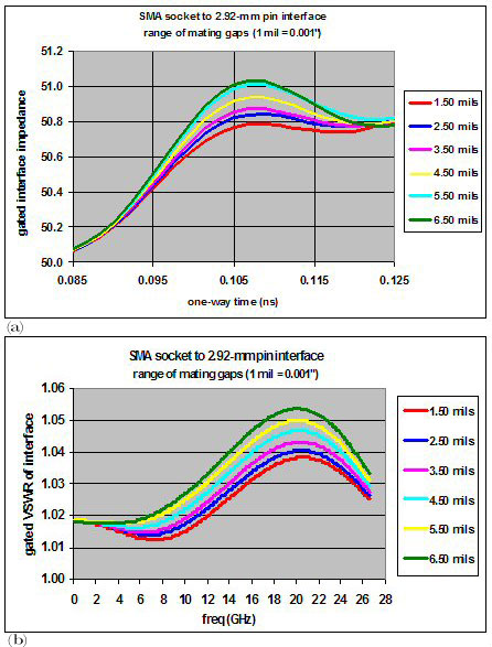
Figure 6B illustrates gated VSWR performance over the range of various center contact gaps. Note that the best VSWR performance occurs at a center contact gap of 2.65 mils, which also produced the smallest impedance discontinuity as evidenced in Figure 6A.
Test Data: SMA-to-2.92 mm Mated Pair
Figure 7A displays the time domain gated impedance response of the SMA-to-2.92 mm connection. The initial impedance is inductive, then increases inductively as gap widens. The reason for this inductive behavior is transitioning from full density PTFE within the SMA to the air dielectric of the 2.92 mm interface.
Figure 7B illustrates gated VSWR performance over the range of the SMA-to-2.92 mm contact gaps. Note the best VSWR performance occurs at a minimum center contact gap of 1.50 mils, which also produced the smallest impedance discontinuity as evidenced in Figure 7A. The VSWR and impedance data tell us this particular interface is primarily inductive. By reducing the center contact gap, the interface is being compensated, going more and more capacitive to offset the interface’s inductive tendency.
| |