

The last 30 years have seen a dramatic increase in data traffic across all wireless networks. This increase has been fueled by video streaming, social networks, online gaming and soon, generative AI with its multitude of expected new applications. Smartphones, infrastructure networks, including small cells, Wi-Fi and fixed wireless access (FWA) all must innovate to stay ahead of the curve.
After three years of decline, smartphone sales are rebounding1 with projected year-over-year growth supported by the deployment of 5G SA and 5G Advanced. 6G is anticipated around 2030, leveraging new frequency bands, known as FR3, between 6 and 15 GHz. Meanwhile, Wi-Fi is entering its seventh generation with the addition of the 6 GHz band and other innovations supporting higher data rates. A planned eighth generation will include an extension to mmWave bands. Forecasters say that Wi-Fi 7 is on track to surpass Wi-Fi 6 by 2027.2
FWA is poised to replace some cable/fiber-optic deployments.3 At the end of 2024, FWA data traffic represented 25 percent of the global mobile network data traffic and this is poised to quadruple by 2030. Unlike mobile wireless, where the user’s location must be tracked geographically, FWA uses fixed consumer premises equipment (CPE) to deliver broadband internet to a home or business. When a line-of-sight link between the base station and the CPE can be established, the complex propagation challenges of the FR2 frequency band at 28 to 39 GHz can be overcome by using high gain antennas and higher power amplifiers (PAs). This FR2 frequency range has the bandwidth to enable FWA to provide a genuine alternative to cable and fiber-optic networks.
While these wireless access technologies have varying needs and specifications, they share a common element: the radio frequency front-end (RFFE). The RFFE, located between the RF transceiver and the antenna, is a critical component responsible for transmitting and receiving wireless signals. The RFFE comprises several key components, including the PA on the transmit path and a low noise amplifier (LNA) and switches on the receive path. These components must work together seamlessly to ensure efficient signal transmission and reception while minimizing power consumption and maintaining signal integrity. For these applications, the average output power of the RFFE is in the range of 0.25 to 4 W, with peak power up to 10 W. This range of output power compensates for the losses of the filters and switches with the actual value depending on the signal bandwidth, QAM modulation, frequency, interference and other factors.
While GaAs was the dominant technology used for the PA, switch and LNA for the first 20 years of mobile cellphone and Wi-Fi applications, it has been progressively displaced by silicon-on-insulator (SOI) technology. This shift to SOI has primarily occurred in the switch and LNA functions, leaving the PA function to GaAs HBT technology for high-power, sub-6 GHz applications and GaAs pHEMT technology for low-power applications in the 6 to 40 GHz frequency range. However, with the progressive shift to higher frequencies, as evidenced by applications in the FR3 band and Wi-Fi 7 with similar or higher transmit power demands, GaAs HBT technology is falling short in power efficiency and this poses a clear challenge to the industry.
5 V GAN-ON-SI E-MODE: A POWERFUL SOLUTION
Enhancement-mode (E-mode) GaN-on-Si offers a compelling alternative to GaAs in 5 V applications due to its unique properties. Produced in a state-of-the-art 8-in. silicon foundry, Finwave Semiconductor’s GaN-on-Si leverages a cost-effective supply chain to deliver cutting-edge technology. From a performance and process control perspective, 8-in tools offer advantages over 6-in. tools in addition to the cost reduction realized by fabricating more devices per wafer.
Unlike mainstream depletion-mode (D-mode) GaN, which requires biasing and sequencing of the negative gate voltage with the drain voltage, E-mode GaN is “normally off.” This means the device requires a positive gate voltage to turn on and, therefore, does not need to be sequenced with the drain voltage. This eliminates the need for a bias controller, which significantly simplifies the application, reduces the die size and lowers cost.
GAN-ON-SI ADVANTAGES OVER GAAS HBT
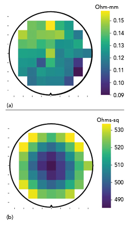
Figure 1 Wafer map of contact resistance, Rc (a) and sheet resistance, Rsh (b).
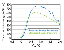
Figure 2 Transconductance versus Vgs.
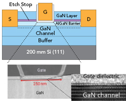
Figure 3 Transistor structure and TEM of gate dielectric interface.
As Finwave has developed the E-mode GaN-on-Si process, several advantages have become apparent:
- Higher breakdown voltage: GaN can withstand higher voltages than GaAs, making it more robust and reliable. This is important for handling signal fluctuations and preventing device damage.
- Better gain and efficiency at higher frequencies: GaN maintains good power efficiency up to 40 GHz. This is crucial for supporting all frequency bands in use and proposed for mobile and FWA (FR1 to FR2 and FR3), Wi-Fi 7 and Wi-Fi 8 (2.4, 5 and 6 GHz, along with mmWave bands).
- Lower cost: GaN-on-Si is becoming increasingly cost-competitive with GaAs, thanks to advancements in manufacturing. This makes it a more affordable option for cellphone manufacturers.
- Integration: Going to higher frequencies necessitates integrating the switch, LNA and amplifier on the same die for optimal performance. GaN HEMTs generally exhibit good noise figure characteristics due to their high electron mobility and low parasitic capacitances, which contribute to the lower noise generation required for LNAs. Additionally, GaN HEMTs offer very fast switching speeds and low insertion loss in an SPDT configuration.
Finwave’s E-mode RF transistor technology has fully realized the advantages of GaN-on-Si, demonstrating the capability of the technology to meet these evolving market demands. Fabricated with a CMOS-compatible process on 200 mm GaN-on-Si wafers, this technology is currently in the process of being transferred to GlobalFoundries for mass production, leveraging their facility in Burlington, Vt. Finwave’s proprietary approach has several innovations that result in record performance and excellent manufacturability, including regrown N++ ohmic contacts with a structure to improve source resistance further, as well as an etch-stop epitaxy structure allowing for highly repeatable fabrication processes with high uniformity.
Excellent Contact and Source Resistance
Finwave’s RF devices employ regrown, heavily doped contacts to achieve excellent contact resistance. Figure 1a shows a wafer map of transfer length method (TLM) measurements for contact resistance on a 200 mm GaN-on-Si wafer. A median contact resistance of 0.126 Ohm-mm was achieved with a cross-wafer standard deviation of 10 percent. Figure 1b shows TLM measurements of sheet resistance on the 200 mm GaN-on-Si wafer.
In addition to the low contact resistance, a proprietary method is used to further reduce the source resistance by about 50 percent compared to a standard GaN device structure. The source resistance is a key device parameter that drives performance in RF transistors used in all parts of the RFFE. Aside from simply contributing to on-resistance (Rds-on), the source resistance acts as a feedback resistor when the transistor is used as an amplifier. The result is that in the linear region, the effective transconductance (gm) is reduced by the factor shown in Equation 1:

Where:
gme is the effective gm
gmi is the intrinsic device transconductance (a theoretical maximum value for gm if the source resistance is reduced to 0)
Figure 2 shows a comparison of transconductance, gm, versus Vgs for the Finwave device with reduced source resistance and a standard device. As shown, the device with reduced source resistance shows a gm peak of 760 mS/mm, while a standard device structure with higher source resistance has a gm peak of 620 mS/mm. Small-signal RF measurements show that the devices with reduced source resistance and higher transconductance have an RF gain that is approximately 0.5 dB higher between 5 and 8.5 GHz and more than 1 dB higher between 8.5 and 24 GHz.
When configured as a switch, the low contact and source/drain resistances directly contribute to the figure of merit, Ron*Coff. While not presented here in detail, initial switch designs with Finwave’s process yielded a figure of merit of 140 femtoseconds, better than typical values for GaAs and approaching those achieved with SOI.4 GaN has the additional advantage of higher intrinsic breakdown voltage and, thus, improved power handling than either incumbent technology. Finally, this RF switch was fabricated using a process optimized for amplifier transistors, with the possibility of use in a fully integrated RFFE. This figure of merit could likely be improved in a process optimized for RF switches.
Etch-Stop Technology
Figure 3 shows a TEM image of the 250 nm Lg and gate dielectric interface, along with the transistor structure. Finwave’s GaN-on-Si epitaxial wafers contain an etch-stop layer, which facilitates the formation of an E-mode channel and ohmic contacts in a highly reproducible way. Instead of relying on a tightly controlled etch rate and time to etch a specific depth into the AlGaN barrier layer to achieve the target transistor properties, the channel etch can land on the etch-stop layer in a controllable way. By using an etch process selective to our etch-stop layer to remove the GaN cap layer over the gate region, we can achieve a low-damage gate recess and a high-mobility channel. This comes with the additional benefit of excellent across-wafer uniformity, including a standard deviation in the on-resistance of 3 percent and threshold voltage less than 100 mV, both with room to improve as we scale toward full production.