


Device Reliability
Reliability is a challenge for GaN-on-Si MISHEMT devices. One of the key issues is the gate dielectric reliability and its effect on the bias temperature instability (BTI). Defects within the gate dielectric bulk material and at the semiconductor-dielectric interface are both able to trap charges, causing Vth, Ron and other device parameter shifts.5 Finwave’s device achieves excellent gate reliability through the optimization of device design and process conditions. High-temperature gate bias (HTGB) stress tests conducted at 150°C with Vg = 1 V, Vd = 0 V for 10,000 seconds show minimal shifts in all device parameters, with a Vth change of less than 50 mV and Ron change less than 0.2 percent. This state-of-the-art reliability performance is achieved by minimizing the effect of the deep traps in the gate region with a high-quality dielectric and low-defect interface. This is critical to enable our technology to operate stably for various RF applications over their lifetime.
DEVICE RESULTS
Figure 4a shows DC measurements at 600 ns pulsed IV. Figure 4b shows the same FET with subthreshold Id-Vgs measurement at Vds = 50 mA and 5 V and transconductance measured at Vds = 5 V. Figure 4c shows breakdown voltage measurements of the FET at different Vgs bias voltages. Destructive breakdown occurs at around 30 V. All these devices are 2-finger RF transistors with a source-to-drain distance (Lsd) of 700 nm, gate length (Lg) of 250 nm and width (Wg) of 50 μm per finger. These were fabricated using standard CMOS-compatible processes and materials, including the passivation and gate dielectrics, as well as the gate, ohmic and interconnect metal layers.
The E-mode FET has a knee voltage, Vknee, around 1 V, on-resistance, Ron, of 0.8 to 0.9 Ohm-mm, peak transconductance, gm, of 760 mS/mm and a threshold voltage, Vth, around 0.15 V. Pulsed-IV measurements reveal excellent dynamic behavior and minimal trapping, with current collapse less than 10 percent around the Vknee voltage. The device has a subthreshold swing of 80 mV/dec and a negligible DIBL of 40 mV/V, demonstrating an MIS interface with very low interface state density.
The DC breakdown voltage was measured at Vgs = -1, -2 and -3 V on the same device. Drain-to-source punch-through was observed for Vgs = -1 and -2 V, resulting in non-destructive soft breakdown behavior. Destructive breakdown occurs at Vds = 30 V and Vgs = -3 V and it is caused by gate dielectric reverse breakdown, resulting in a permanent increase of gate leakage. The off-state leakage of the transistor is typically less than 1 uA/mm, orders of magnitude lower than the conventional Schottky-gate D-mode GaN FETs.6
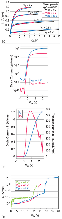
Figure 4 DC measurements of the 2 x 50 μm Lg = 0.25 μm FET.
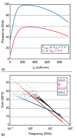
Figure 5 Small-signal FET measurements.
RF Characteristics
Figure 5a shows Ft and Fmax as a function of Id. Figure 5b shows RF gain versus frequency at Id = 300 mA/mm and Vds = 5 V. These small-signal measurements were made on the same 2 × 50 μm, Lg = 0.25 μm FET used for the DC measurements. The results show that extracted Ft is typically between 60 to 65 GHz and Fmax is between 100 and 110 GHz. Fmax is limited by the relatively high gate resistance of the thin Al gate metal which can be improved with standard CMOS back-end processing like copper-based interconnects.
Large-signal load-pull measurements were conducted on the 2 × 50 μm, Lg = 0.25 μm FET at 8, 13 and 26 GHz, covering the proposed usage range of the FR3 band. Figure 6a shows transducer gain and PAE versus Pout at 8, 13 and 26 GHz with Vdd = 5 V. Figure 6b shows load-pull with Vdd of 1 to 5 V at 8 GHz and Figure 6c shows 8 GHz AM-PM within 1.5 degrees for AM-AM within 3.5 dB and Vdd from 2 to 5 V.
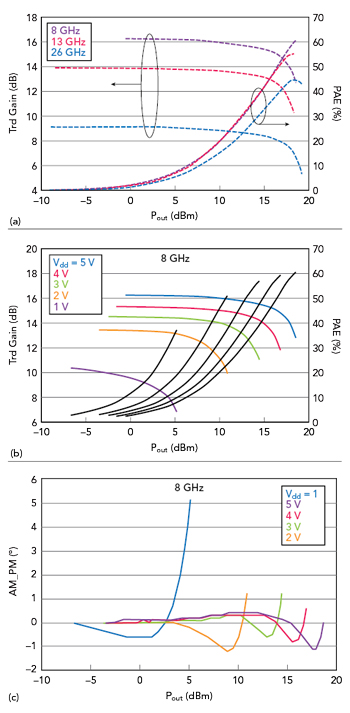
Figure 6 Large-signal FET measurements.
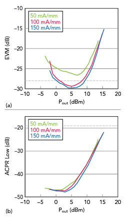
Figure 7 EVM (a) and ACPR (b) at three different Idq bias currents.
The source and load impedances at the fundamental frequency were tuned for maximum PAE, while the impedances at the second and third harmonics were both set to 50 Ohms. The FET demonstrated 16 dB and 14 dB transducer gain with PAE of 62 percent and 56 percent at 8 GHz and 13 GHz, respectively. At 26 GHz, the device gain and PAE are reduced to 9 dB and 45 percent due to the limitation of the relatively large Lg and gate resistance. By reducing Lg and Wg to 220 nm and 2 × 20 μm, respectively, the high frequency performance improves to a gain of 12 dB and 51 percent PAE at 26 GHz.
With the device’s low Ron and Vknee, operation is possible at low Vdd, which is important in envelope-tracking applications. Load-pull measurements were performed with Vdd stepped from 1 to 5 V, with a constant impedance determined to be optimal at a Vdd of 5 V. Device gain and PAE remained high, above 13 dB and 50 percent, respectively, when Vdd was reduced to 2 V. The device also demonstrated good linearity in this range of operation, with AM-PM within 1.5 degrees for AM-AM compression up to 3.5 dB at Vdd of 2 to 5 V.
With a DC breakdown voltage greater than 20 V, the GaN FET is capable of operating at a Vdd higher than 5 V. For example, measurements at Vdd = 8 V showed a gain of 17 dB and PAE of 60 percent at 8 GHz with a Pout of 21 dBm. The resulting power density of more than 1.25 W/mm demonstrates the advantage of GaN over GaAs for higher Vdd and power density.
The high DC breakdown voltage and soft breakdown characteristics result in excellent device robustness to sub-optimal RF conditions. A stress test was performed with a VSWR of 10:1 with Vdd = 5 V. The device was exposed to loads of |Γ| = 0.9 moved around the Smith chart for 30 minutes. Following a cooldown period, large-signal measurements showed no shifts in device performance.
LINEARITY OF BROADBAND MODULATED SIGNAL
Of the many specifications a PA must meet, linearity is the most critical to ensure compliance with 3GPP standards.7 Using a mixed-signal active load-pull system, the fundamental and baseband impedances of the source and load were matched for optimum linearity and efficiency. Figure 7a shows the measured error vector magnitude (EVM) and Figure 7b shows the adjacent channel leakage ratio (ACLR). Both measurements were made using a 5G 64-QAM modulated signal with 100 MHz bandwidth and 7.5 dB PAPR. 3GPP specification target values are shown with a dotted line in the graphs. These measurements demonstrate that the Finwave MISHEMT GaN-on-Si E-mode device can exceed the linearity specifications for Idq values between 50 and 150 mA/mm. Further improvements are expected in devices that are optimized for baseband decoupling.
CONCLUSION
As the wireless communications market continues to demand higher frequency and higher power devices to meet a growing list of high bandwidth applications, new technology is required to deliver the right balance of high performance and low cost to meet these demands. Finwave’s CMOS-compatible E-mode 200 mm GaN-on-Si process meets these challenges. By using existing silicon foundries, this technology can quickly scale to meet the fast production cycle and high volumes required by the handset market. Finally, Finwave’s versatile technology can produce different components needed for the RFFE. It can, therefore, be used to create highly-integrated, high performance, compact and cost-effective RFFE modules.
References
- “Ericsson Mobility Report,” Ericsson, 2024.
- P. S. C. C. G. L. Claus Hetting, Interviewee, Evolution of Wi-Fi 7 Devices: Market Outlook, Innovations in XR, & more. [Interview]. 11 March 2024.
- “Fixed Wireless Access Handbook 2025,” Ericsson, 2025.
- B. Baxter, “Why SOI? Marki Enters the Silicon World,” Marki Microwave, 2022.
- G. Meneghesso, M. Meneghini, I. Rossetto, D. Bisi, S. Stoffels, M. Van Hove, S. Descoutere and E. Zanoni, “Reliability and Parasitic Issues in GaN-based Power HEMTs: A Review,” Semiconductor Science and Technology, 2016.
- V. Johnson, Z. Pogrebin, M. Dipsey, H. S. Emmer, Z. Yuxuan, D. Pei and B. Lu, “200-mm Enhancement-mode Low-knee-voltage GaN-on-Si MISFETs for High-frequency Handset Applications,” CS Mantech, 2024.
- 3GPP, “Technical Specification on User Equipment Radio Transmission and Reception TS 38.101-1 V19.0.0,” 2024.