
Dividing the RAM into two sections provides a simple example. Section 1 contains beam positions 0 to 60 and Section 2 contains beam positions 61 to 120. Initially, start and stop pointer values are set to 0 and 60, respectively. Beam data is also clocked into beam positions 0 to 60 and beam position 0 is loaded. The beam is advanced from positions 0 to 60 several times (the sequencer wraps around and loads the start beam position after the stop beam position). In between beam advances of Section 1, Section 2 beam data is loaded.
When ready to switch from Section 1 data to Section 2 data, a new stop pointer value must be set. To ensure a smooth transition between beam positions 60 and 61, the new stop pointer must be written when the sequencer is at beam position 58 or before. On the first sequence through beam positions 61 to 120, a new start pointer value must be written. The new start pointer value must be set when the sequencer is at beam position 118 or before, or a smooth transition to beam position 61 will not occur. In general, any new beam data or new pointer values should be clocked in two beam positions ahead of the active beam position. Writing new data and then switching back to Section 1 memory can be achieved using the same technique as outlined.
POWER MANAGEMENT
Planar phased arrays that feature BFICs and Tx/Rx modules usually require several different supply voltage domains. Additional supply domains may be required for support circuitry for the BFIC and Tx/Rx modules. These may include a low voltage digital supply and/or an intermediate step-down voltage to feed required supply domains.
For the power tree design, a common voltage such as 12 V is usually chosen to feed all the power management blocks. Common voltage rails of +5 and +3.3 V can be generated easily and efficiently, as well as the common negative counterpart voltage rails of -5 and -3.3 V. PAs and LNAs that use depletion mode field-effect transistor devices often require their gates to be biased to a negative voltage before bringing up the drain voltage to prevent damage to the device. Proper sequencing of the drain and gate voltages is crucial and must be considered when designing the power management circuitry.
Design of Power Management Tree
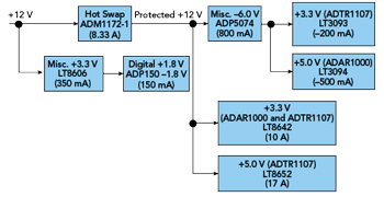
Figure 5 Power tree for a planar phased array system with BFICs and TR modules.
Figure 5 shows the power tree that was used to provide supply voltages for BFICs and Tx/Rx modules that are on the planar phased array board shown in Figure 1. The 12 V input drives a hot-swap circuit featuring the ADM1172 hot-swap controller. This controller provides a protected 12 V with an 8.33 mA current limit to the branch of the power tree that powers the ADAR1000 and ADTR1107 ICs.
From the protected 12 V, the 3.3 and 5 V supplies powering the ADAR1000 and ADTR1107 are generated by the LT8642 and the LT8652, a pair of synchronous step-down Silent Switcher® regulators. These regulators ensure low noise and low spurious tones on critical RF supplies. The LT8642 provides 3.3 V for the ADAR1000’s main supply and the VDD for the switch and LNA of the ADTR1107, while the LT8652 provides the 5 V VDD for the ADTR1107 PA.
To generate the negative supply voltages needed by the ADAR1000 and ADTR1107, an intermediate -6 V negative supply is generated from the protected 12 V rail, using the ADP5074 DC-to-DC inverting regulator. The ADP5074 drives the LT3093 and LT3094 negative linear regulators in parallel. This generates the -3.3 V for the ADTR1107 switch VSS and the -5 V for the ADAR1000.
A secondary branch off the 12 V input powers the LT8606 step-down switching regulator and the ADP150 linear regulator that provides a separate miscellaneous 3.3 V supply and a 1.8 V digital supply, respectively.
Power-Up Supply Sequencing
Powering up the tree shown in Figure 5 is complex. It requires the user to input specific control signals at specific times during the overall power-up sequence. The critical control signal sequencing is described in Figure 6.
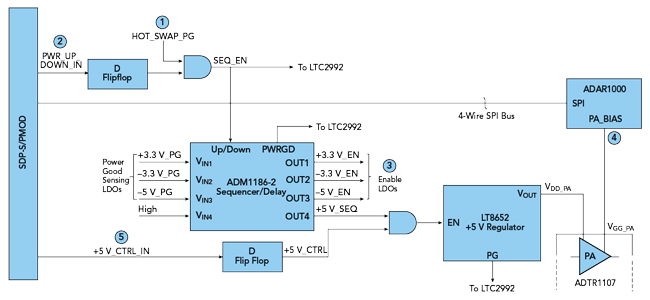
Figure 6 Power-up sequencing for ADTR1107 PA protection.
To start the power-up sequence, first, apply the 12 V power to the board and then the following are powered up:
- The 3.3 V miscellaneous and 1.8 V digital supplies from LT8606 and ADP150 turn on immediately
- Once the ADM1172 hot-swap gives its power good signal (HOT_SWAP_PG, Control Signal 1 in Figure 6), the ADP5074 turns on and provides its -6 V negative rail. Powering up the LT8606, ADP150 and ADP5074 is done automatically and requires no input from the user.
Second, the remaining regulators power up in a specific sequence so that the ADTR1107 PA is not damaged. The sequence is initiated by providing a rising-edge power-up signal (POWER_UP_DOWN_IN, Control Signal 2 in Figure 6) to a D-flip-flop, which holds a high state at its output. The D-flip-flop output is AND’ed with the hot-swap power good signal. If both signals are high, then the sequencer-enable (SEQ_EN) signal is asserted high on the ADM1186-2. The ADM1186-2 allows each linear and low-dropout (LDO) regulator 47 ms for power-up (otherwise a fault condition is raised). An additional 2.2 ms of delay is inserted between each LDO regulator power-up. The exact LDO regulator enable sequence is:
- The ADM1186-2’s OUT1 pin (Control Signal 3 in Figure 13) asserts high and drives the LT8642 3.3 V LDO regulator-enable pin. The LT8642 has 47 ms to assert its power good signal to the ADM1186-2’s VIN1 pin, after which a delay of 2.2 ms occurs.
- The ADM1186-2’s OUT2 pin asserts high and drives the LT3093 -3.3 V LDO regulator-enable pin. The LT3093 has 47 ms to assert its power good signal to the ADM1186-2’s VIN2 pin, after which a delay of 2.2 ms occurs.
- The ADM1186-2’s OUT3 pin asserts high and drives the LT3094 –5 V LDO regulator-enable pin. The LT3094 has 47 ms to assert its power good signal to the ADM1186-2’s VIN3 pin, after which a delay of 2.2 ms occurs.
- The ADM1186-2’s OUT4 pin asserts high and drives an AND gate whose other input is a 5 V control signal. The ADM8611-2’s PWDGD pin will then assert high. The ADAR1000 is now completely powered up along with the ADTR1107 switch and LNA.
Third, the ADAR1000 is programmed for -2 V PA bias outputs (Control Signal 4 in Figure 6), which is a safe value for the ADTR1107 PA during its +5 V power-up. Once all the PA bias outputs are programmed, a rising-edge 5 V control signal (5 V_CTRL_IN, Control Signal 5 in Figure 6) drives a D-flip-flop, which holds a high state at its output. The flip-flop drives an AND gate whose other input is the ADM1186-2’s OUT4 pin. The AND gate drives the LT8652 5 V regulator-enable pin high and starts up the last supply rail. The overall power-up sequencing solution is shown in Figure 6.
Power Monitoring
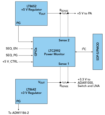
Figure 7 Power monitoring of 5 V and 3.3 V regulators and digital signal sensing.
The LTC2992 monitors the DC power delivered by the LT8642 and LT8652 regulators. The power is monitored by measuring the voltage across a sense resistor on each regulator output. The voltage is sampled with an on-chip analog to digital converter and can be readback via the I2C port.
The LTC2992 also has four GPIO pins, which can be used to sense the state of digital signals. The four digital signals sensed are:
- Power good signal from the LT8652
- The sequencer-enable signal that drives the ADM1186-2 UP/DOWN pin
- The sequencer power good signal from the ADM1186-2
- The 5 V control signal (5 V_CTRL) that enables the LT8652 regulator. The state of the GPIO pins can also be readback over the I2C port. The power monitoring solution can be seen in Figure 7.
The power monitoring and digital signal sensing that the LTC2992 provides help to ensure that the main supplies to the ADAR1000 and ADTR1107 are functioning properly. The power monitoring can also serve as a debug tool and built-in test for the ADAR1000 and ADTR1107 chips themselves. Individual chips in the array can be isolated and powered up to make sure that they are consuming the correct amount of power.
The GPIO sensing of the LTC2992 informs the user if the LT8652 has powered up properly by sensing its power good signal. With this, users can ensure that the 5 V control signal is low until they are ready for 5 V power-up on the ADTR1107 PAs. The GPIO sensing also gives the sequencing state of the ADM1186-2 by sensing whether the LDO regulators are powering up or powering down and if the power-up/down sequence is complete.
CONCLUSION
This application note has discussed some of the challenges associated with designing the RF front-end of a planar phased array system. The size restrictions that stem from the required lattice spacing at high frequencies demand novel approaches to circuit and heat sink design and these challenges have been discussed in a companion article appearing in the March Microwave Journal (J. Dobler and S. Ringwood, “Overcoming Planar Phased Array Circuit Design Challenges,” Microwave Journal, Vol. 66, No. 3, pp. 48-56.). To address all these challenges, most phased array radar systems use BFICs and Tx/Rx modules that interface easily and while this architecture enables shorter RF traces and fewer control lines, it creates timing, control and power management challenges. This application note has described these challenges, along with a power management tree and sequencing scheme resulting in systems with fast responses that are easier to calibrate. Simple single-pin controls and on-chip memory of the BFIC enable quick Tx/Rx transitions and beam advance. This RF front-end power management solution minimizes noise and spurs and avoids amplifier damage.