
Editor’s Note: This application note describes signaling and timing methods, along with power management architectures used in planar phased arrays. In a companion article entitled “Overcoming Planar Phased Array Circuit Design Challenges,” published in the March 2023 issue of Microwave Journal, the authors discuss the PCB and thermal design and layout challenges associated with the digital and RF circuitry used in planar phased arrays.
Two-dimensional planar phased array systems, where the RF circuitry and the antenna elements are on the opposite sides of the same PCB as shown in Figure 1, offer a significant size advantage over 3-D blade-style structures. But that size advantage brings layout, power management and thermal challenges in addition to the traditional timing design challenges associated with radar systems. This application note discusses the signaling and timing methods to control power amplifier (PA) and low noise amplifier (LNA) biasing, transmit (Tx) and receive (Rx) switching, memory loading and beam advance in planar phased arrays. The power management design for the RF front-end is explained, including the power tree and the specific bias sequencing required to avoid PA damage.
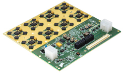
Figure 1 A planar phased array front-end prototyping board (component side).
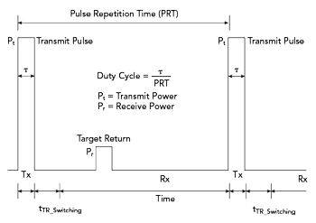
Figure 2 Simplified radar timing.
RADAR SYSTEM DESIGN AND TIMING
In modern phased array radars, the variable phase and amplitude blocks are consolidated into a beamformer integrated circuit (BFIC), with each BFIC containing several variable amplitude and phase blocks. Also, the PA, LNA and Tx/Rx switch can be integrated into a single Tx/Rx module and be optimally designed to work directly with the BFIC.
A monostatic pulse radar has two critical timing characteristics: the transmit pulse duration (τ) and the pulse repetition time (PRT), which is the time between transmit pulses. Modern radars have transmit pulse durations that range between 10 and 100 μs. However, some applications feature pulse durations as short as 500 ns. Typical rise and fall times are between 500 ns and 1 μs and transmit duty cycles are between 1 and 20 percent. Typical pulsed radar timing is illustrated in Figure 2.
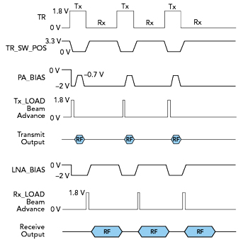
Figure 3 Transmit and receive timing with RF signaling, switch control and amplifier bias.
Radar metrics such as the minimum measurement range (RMIN) or blind range, range resolution and hits-per-scan are directly proportionally to τ and PRT. The minimum measurement range is also directly proportional to Tx-to-Rx switching time:

Minimizing Tx-to-Rx switching time is critical in search radar where targets can be relatively close to the transmitter. Monostatic phased array radar oftentimes is a half-duplex system. Tx-to-Rx switching is accomplished with several control signals that must be sequenced together. These control signals perform the following functions:
- Toggle the Tx/Rx switch
- Enable and disable the PA
- Enable and disable the LNA
- Enable and disable the BFIC’s Tx and Rx paths.
When the beam direction changes, new beam weights must be loaded into the variable amplitude and phase blocks. If local on-chip memory is available to store multiple sets of beam weights, the beam advance can be initiated with a single pulse of a control pin and with no SPI writes. An example of the sequencing and voltage levels of these controls is shown in Figure 3.
An example of real-world control signaling and interfacing is shown in Figure 4. A single channel of the ADAR1000 BFIC is shown connected to a single ADTR1107 Tx/Rx module. The two chips feature a single Tx/Rx control signal going to the ADAR1000 via the Tx/Rx pin. This pin, in turn, controls the PA bias, LNA bias and the Tx/Rx switch on the ADTR1107 Tx/Rx module. It also controls the enabling/disabling of the ADAR1000 internal Tx and Rx beamforming paths. Integrating the Tx/Rx control not only reduces the board layout complexity by eliminating numerous control lines but also enables fast Tx-to-Rx switching times so that metrics like the minimum measurement range are as short as possible.
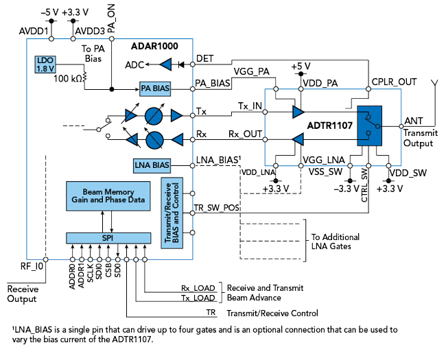
Figure 4 The ADAR1000 and ADTR1107.
BEAM MEMORY
A discrete beamforming solution must apply beam weights from a memory chip to the various variable amplitude and phase shifter blocks. The increased routing complexity and time required to do a beam advance are two major drawbacks of discrete system design. Modern phased array radars using integrated BFICs like the ADAR1000 have on-chip memory requiring a single load pulse and a few additional clock cycles to advance to a new beam. Newer BFICs like the ADAR3000 and ADAR3001 have simplified this to a single pulse with no clock cycles.
In the example shown in Figure 4, the ADAR1000 BFIC features two on-chip locations that can store beam data: registers and random-access memory (RAM). There are advantages and disadvantages to using either type of memory for the storage of beam data. Both types are limited by the maximum SPI clock rate of 25 MHz when writing and reading beam data.
Sourcing beam data from the registers has the advantage of having only enough data for one beam position. That data is directly stored in the registers, meaning there is no need to operate the sequencer or perform any memory fetching. This mode of operation can be important in applications where users do not know what their next beam steering angle is a priori and thus an on-the-fly scheme of writing new beam data needs to be implemented for each new beam steering angle. The downside of using the registers is the time it takes to clock in each new beam position, which is limited by the 25 MHz maximum clock rate. At this clock rate, it takes 4.16 μs to load either a Rx or Tx beam position. Additionally, a quick load command is required to instruct the chip to use the new beam position data in the registers, since the ADAR1000 uses dual-rank registers.
Sourcing data from the RAM is advantageous if the system knows the needed beam steering angles a priori and thus can clock in all the needed beam position data before the active operation of the system. Applications that employ a raster scan like weather and search radars can take advantage of storing beam positions in RAM. The time it takes to clock each beam position into RAM is the same as the registers, but since this is normally done before active operation, the ADAR1000 needs only six clock cycles plus a load command to select a new beam position. This operation takes as little as 320 ns.
RAM Partitioning
If RAM is used to source the beam position data, RAM partitioning can be used to update one section of the RAM while the other section is accessed by the radar controller. Only one section is actively used to source beam position data, while new beam position data is written into the other section(s). This is possible due to the ADAR1000’s use of start and stop RAM pointers, which enable the sequencer to start and stop at any arbitrary beam position in RAM.