

mmWaves are defined as electromagnetic waves with wavelengths from 1 to 10 mm. They belong to the extremely high frequency band of the radio spectrum with a frequency range from 30 to 300 GHz.1 Research and industry are finding the larger bandwidth of mmWave bands attractive, which is increasing the use of these bands in current and emerging RF applications. These bands offer higher data rates and lower latency, which makes them useful for data communication applications like 5G. In addition to communications applications, automotive radars use the 77 GHz band to achieve a better resolution.
5G frequency spectrum is divided into two ranges; frequency range 1 (FR1) consists of the sub-6 GHz bands and frequency range 2 (FR2) covers frequencies above 24 GHz.2 Thanks to its larger available bandwidth, 5G FR2 frequencies allow for higher capacity and faster connectivity in comparison to the FR1 frequencies that older generations of networks use. Densely populated areas like stadiums and factories, along with video streaming services are some of the many application areas where 5G mmWave technology can be especially useful.
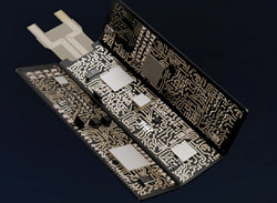
Figure 1 Printed circuit board traces.
Automotive mmWave radars operating in the 76 to 81 GHz band, are widely used in advanced driver assistance systems such as adaptive cruise control, cross-traffic alert and blind spot detection.3 These systems increase the safety and comfort of the drivers, and they are commonly utilized in the automotive industry. Radars are used to measure the range, velocity and angular position of the surrounding cars and obstacles. These radars can be integrated invisibly into the car bodies since the mmWave signals will easily radiate through the body material. This allows for stable target detection even under harsh weather conditions.4
The antennas that radiate or receive electromagnetic energy are one of the key components of communication and radar systems. The performance and size of these radar systems are greatly affected by the design and performance of the antennas. Planar antenna arrays manufactured with printed circuit board (PCB) technology are commonly used in both applications because of their low cost and profile. However, the performance of the antennas can be affected significantly by high dielectric losses. If this occurs, the antennas will provide only moderate gain and efficiency at the mmWave bands. A solution to reduce dielectric loss involves introducing air cavities by removing part of the dielectric material. Typically, these air cavities are formed in the PCB stack-up by laser cutting or by controlled depth milling.
MATERIAL IMPACT ON TRANSMISSION LINE PERFORMANCE
Planar transmission lines are traditionally utilized in PCBs as traces to transmit electrical signals between different components such as resistors, capacitors and ICs, as shown in Figure 1. They are also used to transmit high frequency signals between the IC and RF front-end, where controlling the line impedance is required to minimize signal propagation distortion. The high volume requirements of wireless applications increase the interest in PCB technologies for mmWave applications. Unfortunately, the high loss of the traces at mmWave frequencies reduces the power efficiency and signal integrity significantly. The impedance of the line is determined mainly by the dielectric constant of the material, while the dielectric loss is related to the material’s dissipation factor. As a result, the selection of proper dielectric material is important for PCB and HF designers.
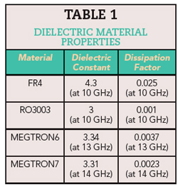
FR4 is one of the most popular materials used in PCB construction. It consists of glass fiber and epoxy resin. Due to its low cost and known electrical and mechanical properties, it is preferred in a wide range of applications where the highest performance is not required. However, it becomes inefficient at mmWave bands because of its high dissipation factor. Furthermore, the dielectric constant can vary considerably across the length and width of the PCB depending on the glass fiber and resin content. This variation causes a degradation in circuit performance. Low loss PTFE materials or materials that contain special resin and glass cloths are used in high frequency applications. In addition to their low dissipation factors, these materials provide a more stable dielectric constant. RO3003 and MEGTRON7 are examples of common high frequency laminates. The dielectric constant and dissipation factor of some representative dielectric materials are given in Table 1.
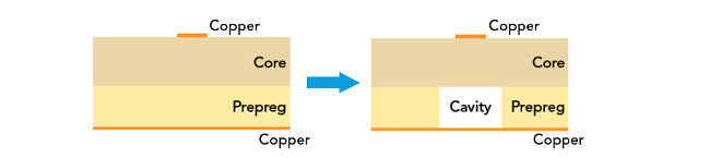
Figure 2 Cross-section of the stack-ups without and with an air cavity.
Microstrip Line Insertion Loss Comparison
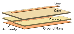
Figure 3 Exploded view of the microstrip line with an air cavity.
A microstrip line consists of a conducting strip, which is printed on a grounded dielectric substrate. Electromagnetic fields occur between the conducting strip and the ground plane. Most of the fields are concentrated inside the dielectric material underneath the line, which causes the atoms to polarize, creating dipole moments.5 Vibration of these dipole moments will create heat and that energy dissipation manifests as dielectric loss. Together with the conductor and radiation loss, dielectric loss contributes to the insertion loss of the line. Dielectric loss is quantified by the dissipation factor or loss tangent of the material. Since air has a dissipation factor ideally of 0, replacing the dielectric material with air reduces the dielectric loss, along with the total insertion loss of the line. Figure 2 illustrates the cross-section of the proposed stack-up that contains an air cavity in the prepreg layer, while Figure 3 shows an exploded view of the material stack.
Figure 4 compares insertion loss for different air cavity dimensions when the dielectric material is FR4. The total stack-up thickness is kept constant at 200 μm for all cases and the traces are simulated at 50 GHz. The red curve at the top corresponds to the conventional microstrip line, without an air cavity. Creating an air cavity in the stack-up with a width of 500 μm and a thickness of 50 μm decreases the insertion loss by 33 percent compared to the basic microstrip line. By increasing the air cavity dimensions further and setting the width to 1300 μm and the thickness to 125 μm, the insertion loss can be reduced by 77 percent. As shown in Figure 5, there is also a considerable reduction in the loss by using RO3003 dielectric material. For the smaller air cavity with a width of 500 μm and a thickness of 50 μm, the insertion loss decreases by 17 percent, while loss decreases by 44 percent for the air cavity with a width of 1300 μm and a thickness of 125 μm. RO3003 is a low loss material with a low dissipation factor, so the reduction of insertion loss created by introducing air cavities should be larger for FR4.
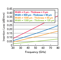
Figure 4 FR4 insertion loss comparison.
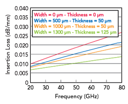
Figure 5 RO3003 insertion loss comparison.
AIR CAVITY-BACKED ANTENNAS
28 GHz Air Cavity-Backed Aperture-Coupled Patch Antennas
An aperture-coupled rectangular patch antenna (ACPA) is a common antenna design for 5G mmWave modules. This type of antenna is typically fabricated using multilayer PCB technology. It includes a patch radiator on the top layer, a feed network on the bottom layer and a ground plane on the middle layer. In the ground, there is an aperture, which acts as a coupler between the feed line and the radiator. In this work, an air cavity is created in the stack-up to improve the antenna performance, as illustrated in Figure 6. The thickness of the air-filled layer in the MEGTRON7 material is two-thirds of the entire antenna substrate. The antenna substrate needs to have a certain thickness of low dielectric constant to obtain good radiation performance. As shown in the performance curves of Figure 7, the stack-up with the air cavity outperforms the other dielectric materials in terms of gain and radiation efficiency.
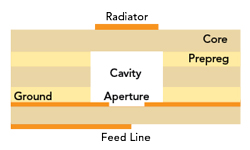
Figure 6 Cross-section of an air cavity-backed aperture-coupled patch antenna.
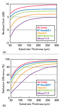
Figure 7 Single patch ACPA performance.