

The mmWave spectrum offers many compelling advantages for communication applications. Compared to microwave systems, mmWave offers larger blocks of less contested and less regulated bandwidth for high data rates. The shorter wavelength allows reduced antenna size for a given antenna gain for compact systems. Compared to optical, mmWave losses in the atmosphere are modest and it is possible to “burn through” inclement weather to maintain a link. Additionally, with enough power the spot size at the receiver can be relatively large, providing tolerance for imperfect antenna pointing accuracy.
Wireless communications systems are finding increasing applications because of their reduced capital costs, ease of deployment and reduced environmental impact over physical carriers such as fiber. Wireless transmitters have long played an essential role in satellite communications (satcom) and are used terrestrially as point-to-point relays to carry backbone traffic where the deployment of physical lines is difficult. Recently mmWave systems have seen rapid adoption for point-to-point terrestrial links up to W-Band and in satcom for gateway uplinks up to V-Band. Access to bandwidth at these frequencies enables competitive data rates with those available over fiber optic cables. Figure 1 shows the large swaths of frequency blocks available with the 71 to 76 GHz and 81 to 86 GHz bands each offering 5 GHz of continuous bandwidth. At W-Band, 92 to 114 GHz and at D-Band, 130 to 174.5 GHz, even larger bandwidths are being considered for near-term network growth.1 Future systems will operate at G-Band frequencies spanning 200 to 300 GHz ranges.2
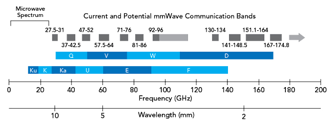
Figure 1 mmWave spectrum bands.
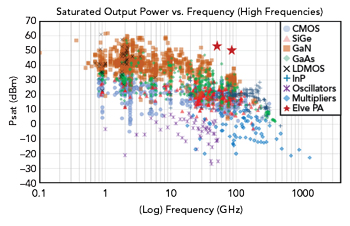
Figure 2 Summary of available SSPAs.3 Elve power amplifiers have been added.
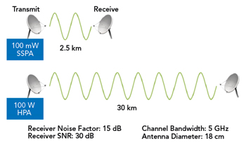
Figure 3 Range enhancement with an E-Band TWT.
The power amplifier (PA) is usually one of the last components in the RF chain before the antenna, playing a key role in system performance. Making use of mmWave for communications and imaging requires acquiring the signal at the receiver with a suitable signal-to-noise ratio. Practical systems that function over appreciable distances in various weather conditions often need tens of watts of power to meet requirements.
Achieving this at mmWave frequencies is a challenge. The advantages of mmWave systems have been acknowledged for decades, but the lack of availability of mmWave PAs has impacted mmWave deployment. Local heat dissipation limits achievable power in a single MMIC, so reaching watts of output power requires power combining that reduces efficiency. Low efficiency, low system-level power density, high thermal load and design complexity of mmWave solid-state power-combined systems are some of the challenges of deploying mmWave systems. While several technologies have been explored to deploy mmWave PAs,3 GaN and GaAs are the solid-state solutions that offer the most potential for high power levels as shown in Figure 2. New technologies offering increased power efficiently in compact forms are needed.
Traveling wave tube (TWT) amplifiers (TWTAs), consisting of a TWT and its power supply, or electronic power conditioner are a well-established highly reliable technology4,5 that has demonstrated high power efficiency in a compact form at mmWave frequencies. We believe that the technology outperforms solid-state power amplifiers (SSPAs), but is often overlooked for deployment in high data rate communications systems. As shown in Figure 3, a 100 W TWTA allows data to be transmitted at the same rate 10x as far as a 100 mW amplifier.
LINEAR BEAM AMPLIFIER OVERVIEW
Many vacuum devices are used to generate or amplify mmWave power. Linear beam devices, such as klystrons, TWTs and backward wave oscillators (BWOs) provide power that is unachievable in solid-state devices. Klystrons are narrowband amplifiers with resonant circuits, producing high peak power. They are used in radar and some communication systems. TWTs employ a non-resonant circuit that allows significantly wider bandwidth, typically at lower power levels than klystrons. BWOs have a circuit that is designed for an unstable interaction with a backward traveling wave so the devices generate RF without an input signal, effectively amplifying noise.
THE TWT
TWTs are the vacuum amplifiers used most commonly in communication systems. Dr. Rudolf Kompfner is credited with the invention of the TWT,6 but Dr. John R. Pierce quickly realized the potential of the device to enable the type of communications he was working on at Bell Laboratories. He developed much of the engineering needed to design and build practical devices.7
TWTs amplify a signal using the kinetic energy carried by electrons traveling in a vacuum environment. The operation starts with an electron gun that creates an electron beam that is electrostatically focused into a narrow stream. Most TWTs employ a thermionic cathode, where a low work function material is heated to emit electrons into the vacuum. The hot cathode evaporates the emissive material, leading to a finite lifetime of electron emission. Electron energies are given by a Maxwellian distribution in the cathode and only those with energies above the cathode work function can travel into the vacuum. Higher electron emission requirements mean a hotter cathode for a given cathode material work function. A voltage applied to the anode accelerates the electrons and lenses electrostatically focus them into a compact beam. If the cathode surface is large and the focused beam small as in a high frequency TWT, this focusing may reduce the beam’s cross-sectional area by a factor of a hundred, requiring extreme precision in the lenses.
Next, the electron beam, carrying kinetic energy established by the electrostatic acceleration, enters a magnetic field that counteracts the electrostatic repulsion of the electrons, maintaining a constant cross-section as the electrons travel through the interaction circuit. The circuit starts with an RF input port where power is injected. The RF is carried on a transmission line that wraps around the beam so that the electric field from the RF input power is aligned with the electron beam’s axial motion. The alternating electric field speeds up some electrons and slows down others, forming electron bunches. As the modulated electron beam travels with the RF wave, the electron beam induces current on the circuit, causing the amplitude of the circuit wave to grow at the expense of the electron kinetic energy.
The electron beam and the electromagnetic wave must travel at similar speeds to form the electron bunches. Otherwise, the electron sees a sinusoidally-varying electric field with velocity increasing and decreasing, but on average retaining its initial energy. Electrons moving at a similar speed to the wave are continuously accelerated in the accelerating phase and continuously decelerated in the decelerating phase.
The amplified RF is coupled out at the end of the circuit and the spent electron beam goes to a collector. In most TWTs, the collector contains multiple electrodes, each depressed below ground to a different electric potential level. The electrons give up kinetic energy as they climb the potential hill created by these biased electrodes, allowing the power supply to recover energy, significantly improving the overall operating efficiency of the device. This energy recovery is one of the reasons that TWTs can achieve significantly higher efficiency than solid-state amplifiers.
The technique of bunching the beam by adjusting electron velocity with an electromagnetic signal is commonly used in vacuum amplifiers. First demonstrated in klystrons in the 1930s, velocity modulation can produce high gain in the interaction circuit since small changes in velocity result in patterns of high and low current density downstream. Since all this happens in a collisionless vacuum environment, the approach allows these devices to scale to very high frequencies.
The most used TWT circuit is a helix, or more specifically a coaxial transmission line with the center conductor twisted into a helical path. The quasi-TEM mode on the transmission line follows the helical path, causing the axial velocity to slow. The electron beam travels through the center of the helical line where the electric field of the electromagnetic wave acts on the beam along the direction of the beam propagation.
On a coaxial line with a vacuum dielectric, the electromagnetic wave propagates at the speed of light. In a TWT, the helix pitch, the distance between each turn, reduces the electromagnetic wave’s net velocity in the beam direction. Figure 4 shows this with a “dispersion curve,” the relationship between frequency ω=2πf and wavelength. Frequency is plotted on the y-axis and inverse wavelength, called β on the x-axis. Since the velocity of a wave is given by frequency multiplied by wavelength, the velocity at any point on the curve is ω/β .

Figure 4 Dispersion curves for coaxial line and helical delay line.
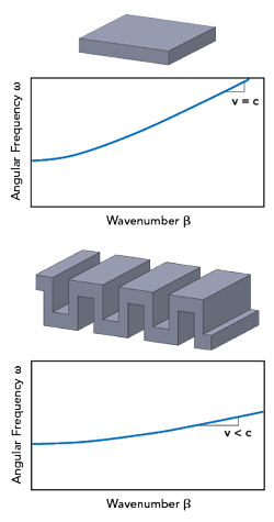
Figure 5 Waveguide and folded-waveguide dispersion diagram.
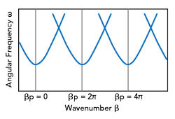
Figure 6 Folded-waveguide periodic dispersion curve.
TWT circuits based on two-conductor transmission lines can be extremely wideband since they use the TEM mode, which has no cutoff frequency. Unfortunately, the center conductor must be electrically isolated from the outer conductor. This requires ceramics to support the helix, resulting in non-ideal heat paths for electrons that intercept the circuit and ohmic losses generated in the helix. For applications requiring smaller bandwidths, single-conductor transmission line circuits are preferable. These circuits can be all metal, improving thermal power handling. Many traditional TWTs are made from coupled cavities that use a series of resonant cavities connected with irises or slots to create a winding RF path.
A folded-waveguide circuit employs a waveguide bent back on itself many times, reducing the effective speed of the RF along the beam propagation.8 A beam tunnel hole is punched through the circuit. Starting with the dispersion curve of the waveguide, the net velocity of the RF following the waveguide path is reduced as shown in Figure 5.
The periodic structure results in a periodic dispersion curve shown in Figure 6. The direction of the electric fields reverses each time the waveguide folds back on itself. As the electron beam passes through the folded-waveguide structure, it sees an additional 180-degree phase shift every half period as shown in Figure 7.
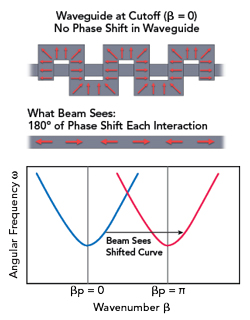
Figure 7 Folded waveguide field as seen by electron beam.
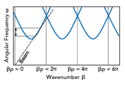
Figure 8 Dispersion curve for folded-waveguide TWT interacting with an electron beam.
Figure 8 shows the resulting dispersion curve. Appropriate values of waveguide cross-section and path can be chosen to achieve a phase velocity that matches the beam velocity. The circuit can be optimized for a relatively constant phase velocity over the band, resulting in flat gain over frequency for a wideband amplifier.