
At frequencies below several GHz, the impact from solder process variations and other fabrication and assembly factors is typically benign when good design practice is used. At tens of GHz, the impact from fabrication and assembly variations becomes significant enough that minimizing tolerances in the signal path is essential for many applications. This is why compression-mount test connectors are becoming an increasingly popular solution for upper mmWave interconnects in test, prototyping and diagnostic applications. Another factor to consider is that compression connectors are also compact, which is advantageous as many upper mmWave applications are also now at far greater levels of interconnect density on boards with shrinking available board space.
However, these connectors are not without their challenges. The compact form factor and necessarily small size results in the potential for misalignment, as the tolerances for these connectors and landing pads are extremely tight. It is entirely possible to misalign coaxial compression connectors without knowing until the test setup is underway and unpredicted test results are observed. Fortunately, there is now a solution to this challenge that provides an easy-to-read visual indication of the proper alignment that speeds up the assembly and alignment of compression connectors.
WHY COMPRESSION CONNECTORS?
There is a growing demand for precision, high frequency test connectors that reach and exceed, 90 GHz bandwidth. This is a result of ever-climbing data rates, such as 224 gigabits per second (Gbps) pulse amplitude modulation 4-level (PAM4) and the increased interest in developing mmWave communication and sensing technologies operating in V-Band (40 to 75 GHz), W-Band (75 to 110 GHz) and beyond. The higher data rates used in backhaul and networking infrastructure necessitate the use of RF test equipment for development, verification and even troubleshooting. Hardware components of mmWave communication and sensing systems, even for devices that operate in the lower portion of V-Band, often need to be tested at many times their maximum operating frequency to capture nonlinear and harmonic performance.
The maximum frequency of a transmission line, be it planar or coaxial, is dictated by the dimensions of the conductors and the spacing between them. To realize higher-frequency transmission lines, the physical geometry of the planar traces and the coaxial conductors in a coaxial connector and cable are necessarily smaller than their lower-frequency counterparts. For some applications, this is advantageous, as it allows for higher levels of interconnect density. An example of this is the multitude of antenna feeds from advanced/active antenna systems operating in the upper mmWave range.
As the physical dimensions of the interconnect shrink, the tolerances associated with interconnect placement and fixturing also need to be tighter, meaning that many alignment strategies that are appropriate for larger interconnects are no longer viable with minute high frequency interconnects.
The Main PCB Surface Trace Interconnect Solution Parameters
- Bandwidth (Hz)
- Insertion loss (dB)
- Return loss (dB)
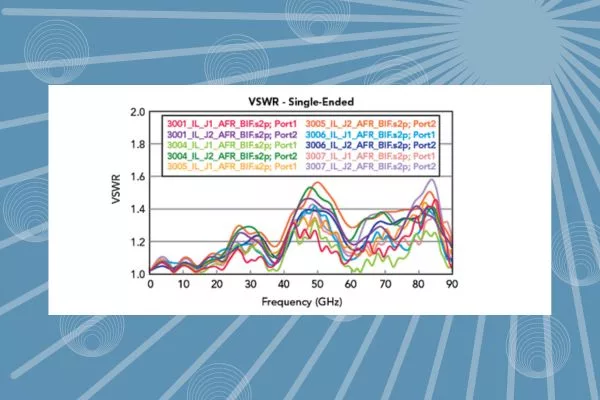
- VSWR
- Impedance (Ω) typically 50 or 100 Ω
- Power handling capability (dB) typically specified for continuous wave and/or peak
- Repeatability
- Ease of use and setup considerations
- Cost
PCB SURFACE TRACE INTERCONNECT SOLUTIONS
There are a variety of high frequency interconnect methods for attaching test and diagnostic equipment to surface traces or landing pads on a PCB, each with benefits and drawbacks. Given the desirability of broadband operation, coaxial interconnect and broadband planar transmission lines are common for these applications. Hence, the interconnect challenge is to ensure reliable, repeatable, high precision connections between minute landing pads of planar transmission lines to the test leads of high frequency test equipment.
The PCB Surface Trace Interconnect Solutions
- Coaxial cable directly soldered to surface planar transmission lines
- Coaxial connectors, either surface, through-hole or edge-mount soldered
- Pre-manufactured or custom single-use solder test leads
- Coaxial probe station
- Compression connectors, either surface or edge-mount
The traditional method is to directly solder a coaxial cable center conductor and outer conductor (shielding) to the landing pads on a board. This is often used to bridge two surface transmission lines or when using half of a coaxial cable assembly to connect surface transmission lines to external equipment. Though this method is functional, the poor tolerances achievable with hand-soldered and hand-prepared coaxial capable cutoff sections means this method is likely to have the lowest precision and repeatability. Depending on the technique used, this method likely will not be suitable for mmWave applications unless performed by a skilled technician with specialized equipment.