

RF systems are critical in modern military applications involving activities such as reconnaissance, communication, navigation, timing, positioning, tracking and detection. Software-defined radio (SDR) is one such system leading the way in how mission-critical defense systems relying on RF technology are implemented. Important military areas where SDRs are crucial include spectrum monitoring and recording, signal intelligence (SIGINT), electronic warfare (EW) and military satellite communications (satcom). Each of these relies on advanced RF and signal processing systems to handle large amounts of data quickly and accurately at relevant portions of the system.
In this article, we discuss how a SDR’s performance must be matched to its intended military or aerospace use case. Important performance specifications of the radio front-end (RFE) and digital back-end (DBE) include tuning range, instantaneous bandwidth, protocol stack, backhaul bandwidth, dynamic range/sensitivity and MIMO functionality. These are covered, and we discuss why certain performance specification are so important to various military and aerospace applications.
SDR OVERVIEW
An SDR is a transceiver with embedded processing and reconfigurable radio parameters, capable of RF tuning, demodulation and digital processing of the signal, with networking to connect the SDR to an external server for further processing. The functions performed by the SDR were historically done on customized hardware (e.g., equalizers, modulators and coders), without the flexibility offered by the SDR. SDRs range in size and complexity from small, low-power transceivers embedded in sensors and actuators to complex, MIMO systems with high sample rates and data throughput, which are used for spectrum monitoring.
High performance SDRs contain five functional elements, often designed as modular boards: digital, power, receive (Rx), transmit (Tx) and timing (see Figure 1). The timing provides clocking for the analog-to-digital converters (ADC), digital-to-analog converters (DAC) and local oscillators (LO) for up- and down-conversion. A generic SDR has three stages: RFE, DBE and a mixed-signal interface (MSI), which is essentially the connection between the DBE and RFE.
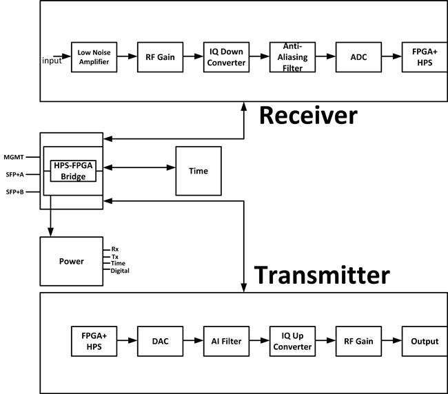
Figure 1 Functional block diagram of SDR.
The RFE has Tx and Rx channels, which can work with signals up to 10s of GHz. The Rx includes multistage signal chains for baseband and higher frequency bands, which include a low noise amplifier (LNA), attenuator, I/Q down-converters, anti-aliasing filter (AAF) and ADCs, leading to the FPGA. Similarly, the Tx chain begins at the FPGA and leads to various frequency ranges (baseband or higher), beginning with the DACs, AAF, frequency synthesizer and LO, I/Q up-converters and RF gain blocks. High performance SDRs tend to include completely independent Tx and Rx chains, and the highest bandwidth and MIMO SDRs provide up to 3 GHz of instantaneous bandwidth per channel and up to 16 independent Rx and Tx signal chains.
The DBE handles the communication protocols, signal processing, data storage, control and intelligence. For ultra-low latency communication, the DBE uses a high-end FPGA with an on-board DSP for modulation, demodulation, data packetization, up- and down-conversion and other application functions such as AI or security. The FPGA sends 10/100 Gbps SFP+/qSFP+ Ethernet packets containing raw I/Q data to a host or network server connected to the SDR. The DBE can be constructed or changed to support new radio protocols and DSP algorithms as well as using the host system for signal processing raw I/Q samples. The MSI is composed of the dedicated DACs and ADCs, which use JESD high speed serial links to interface with the FPGA.
SDR OPERATION
Tuning an SDR for Tx or Rx involves several mechanisms unique to the frequency range of the signal chain, i.e., baseband, low, mid or high band. To illustrate, for transmitting in baseband, the user defines the sample rate on the application before generating samples on the FPGA. Once the samples are generated, interpolation obtains a bandwidth that is an integer multiple of the DAC clock. Interpolation is critical for the next step: using a CORDIC mixer on an FPGA for digital up-conversion. This increases the signal frequency and causes images, signals at a frequency not within our bandwidth. The DAC then converts the digital data to an analog signal, and the AAF eliminates the image signals and reduces the DAC bandwidth by 80 percent. Finally, the “clean” analog signal is amplified and connected to an external power amplifier and antenna.
On the Rx side, the signal received by an external antenna is amplified by an LNA in the SDR and filtered with a lowpass filter. An AAF limits the spectrum to within approximately 80 percent of the converter’s bandwidth to ensure no undesirable or alias signals. An ADC then converts the analog signal to digital and passes the digital data over JESD serial links to the FPGA for digital down-conversion using a CORDIC mixer. The user-defined sample rate sets the bandwidth, and decimation is used to ensure the received signals fall within this bandwidth. The sampled data can be sent over Ethernet to the host system for further processing.