

A simple formula for calculating the ENOB due to jitter is2

For example, if the incoming sine wave is 20 GHz and the RMS jitter is 50 femtoseconds, then the fractional period of jitter is 1/1000, and the ENOB due to jitter is 7 bits.
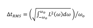
Given a phase noise spectral density L(ω) around the sampling frequency of the clock, the period jitter is simply the square root of the integrated double-sided phase noise power divided by the sampling frequency ω0 in radians per second.
The phase noise at frequencies below 10 kHz offset from an oscillator’s frequency typically has a lowpass slope of 1/ƒ2 transitioning to a 1/ƒ slope from 10 kHz out to around 10 MHz, depending on the design of the oscillator. Beyond 10 MHz offset, the phase noise power density flattens out and has an effective bandwidth well beyond the sample rate, because the sample clock must have a bandwidth many times higher than the sample frequency to have a sharp-enough edge for sampling. Consequently, in wideband samplers, the accumulated wideband phase noise usually dominates the relatively small amount of narrowband close-in phase noise near the oscillator frequency. All the high frequency components of phase noise beyond the sampling frequency are effectively aliased into the baseband of the ADC.
Because RF receiver design must include a noise figure (NF) analysis of the entire receiver chain, the NF of the ADC must be determined so that an adequate amount of gain is placed in front of the ADC. For an ADC, the NF is defined as the ratio of the total effective input noise power of the ADC to the amount of that noise power caused by the source resistance alone. Because the impedance is matched, the square of the voltage noise can be used instead of noise power.
ADCs have relatively high NFs compared to other RF parts, such as low noise amplifiers (LNA) or mixers. In an actual system application, however, the ADC is typically preceded by at least one low noise gain block which reduces the overall ADC noise contribution to a very small level.
For example, an ADC having a full-scale RMS signal input of 1.13 V into 50 Ω will have a +14 dBm input level. If the bandwidth is 40 MHz, then the NF is 30.1 dB. An example from the Analog Devices MT-006 Tutorial3 shows a Friis analysis demonstrating that a 25 dB LNA gain stage having a 4 dB NF in front of the ADC will bring down the net effective cascaded NF to 7.53 dB.
TEST CHALLENGES
Significant testing challenges are presented to both the manufacturer of RF ADCs, and more so to their customers who want to verify performance in their application environments to determine the impact of the RF ADC on their system designs. At such high sample rates, the test equipment needed to verify the manufacturer’s claimed specifications is extremely costly. Bench test equipment costs can easily exceed $1 million USD and require a subject-matter test expert to perform the measurements and obtain reliable data. The expert must also comprehend the impact of the result on the end-system.
Is there a single reliable general parameter such as ENOB or SFDR that is the ultimate dispositive parameter? The simple answer is: ‘No.’ A comprehensive range of parameters for characterization is generally necessary, but each application for which the ADC is used will make certain parameters more important than others.
For example, clock jitter is a determining performance metric that limits the ENOB at frequencies approaching the Nyquist rate. If 7 ENOB requires a 50 femtosecond RMS total jitter budget and that budget requires a sub-50 femtosecond jitter from the system clock source driving the ADC, but the system can only produce a 100 femtosecond jitter sample clock, is that effective loss of 1 bit from 7 to 6 bits acceptable to the customer?
ADC nonlinear distortions are primarily manifested in their INL characteristics, describing deviation from an ideal linear monotonic response. Unfortunately, suppliers specify INL only by the maximum static (DC) deviation in LSB units from the ideal staircase linear response. This single point measure provides very little information on the nature and curvature of the deviation across the full input code range, from which dynamic IMD can be estimated.
When the ADC supplier does not provide specifications for a two-tone test of third-order intermodulation (IM3) characterization, what are customers to do if they then test the ADC for IM3 and third-order input intercept point (IIP3), resulting in an unacceptable IM3 and IIP3 measures? Until recently, most ADC suppliers did not provide in-band IMD characterization, but rather a single tone sine wave testing for out-of-band harmonic distortion. However, RF amplifier or mixer design usually entails characterizing the IIP3 using a two-tone test.7
Most data converter suppliers have, to date, not provided this type of test data to their customers due to their belief that third-order harmonic distortion measures provide the requisite information on the same third-order distortion coefficient that governs in-band IM3. However, owing to the high frequency response roll-off at the third harmonic, thereby creating the appearance of lower third-order distortion, this presumption typically results in underestimating the in-band IM3 distortion.
Admittedly, proper two-tone testing is more exacting than single tone testing. The method requires two very pure and well-isolated RF sources with high Q bandpass filters at each source output to ensure minimum nonlinear parametric cross-modulation components that may be confused with the IM3 tones. While RF engineers are historically well acquainted with these types of test procedures, data conversion suppliers are not. The situation will likely correct itself as RF ADCs become more mainstream.
As newer semiconductor technologies have driven power supply levels down to 1 V, the input buffer or track-and-hold amplifiers at the front end of the ADCs are now exhibiting lower saturation levels. Hence, two-tone distortion measurement methods are becoming essential for characterizing high speed ADCs.
NLEQ FOR ADCS
NLEQ in communication systems design originated in the 1970s or earlier, and became a standard staple in high-performance modems in telecommunications by the early 1990s. The proper use of NLEQ requires characterization of the system exhibiting the nonlinear behavior under specific signal conditions. Modern NLEQ techniques entail an adaptive convergence of the estimates of a Volterra series’ coefficients to mimic the inverse character of the nonlinearities.
Take the simplest example, a single tone test. For simplicity, assume that the nonlinearity of the system is a simple saturation characteristic such as an S-curve of the input/output relationship of an amplifier. Under this odd-symmetry condition, the Volterra coefficients are only a few odd-order coefficients, perhaps the third- and fifth-order, sufficient to cancel odd harmonic distortion components. For this test to be meaningful in the real world, the amplifier in this example would have to exhibit no time-varying characteristic or AC settling time issues that are a function of increasing nonlinearity as the sine wave test increases in frequency. Of course, this is usually not the case.
A single adaptation of the Volterra coefficients to that single tone at that single amplitude may result in a near-perfect cancellation of the harmonic distortion only under those conditions. It may produce a great-looking plot for a data sheet, however! Now, change the amplitude and frequency of incoming tone. One must re-adapt to a new set of Volterra coefficients. The situation gets far more complicated with two-tone testing. Now, the IM3 rises polynomially with incoming tone amplitude.
To find a suitable set of adapted Volterra coefficients, one would need to pre-train the system and come up with a set of best-fit coefficients that reduce the IM3 tones across their amplitude range. It gets more complicated yet with a variable spacing of the two tones a variable center frequency between the tones across the full Nyquist bandwidth of interest. In the above examples, it is assumed that the saturation of the input amplifier is the dominant source of distortion.
An on-chip scheme for linearizing an ADC under a single tone test has been demonstrated by Goodman et al.11 This includes dither injection to train and calibrate errors up to the fifth-order in the digital domain. It has been used in pipeline converters and effectively smooths out INL errors including those occurring at inter-stage breaks. A conceptual block diagram of this scheme is shown in Figure 3. Note that this approach is not all-digital and needs a digital-to-analog converter. It appears to be more accurate at lower frequencies, as it does not account for frequency dependent effects and loses its effectiveness as the input signal frequency is increased.
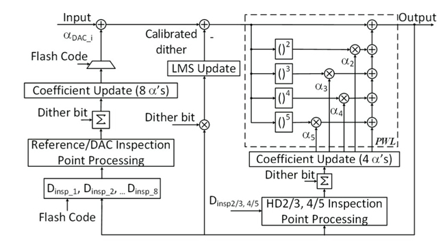
Figure 3 On-chip linearizer.10
Conceptually, what is needed is an all-digital approach, where the digitized RF signal is digitally post distorted and then adaptively correlated in a digital feedback loop with the desired signal. Such an approach would not require dither and would be less frequency dependent. Goodman proposed such a model,11 and a general conceptual diagram is shown in Figure 4.
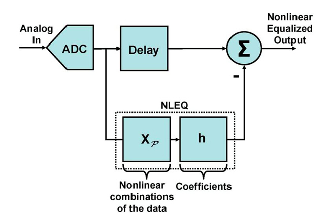
Figure 4 Goodman’s all-digital generalized NLEQ conceptual diagram.11
All the highest frequency RF ADCs are of the interleaving variety. An interleaved ADC is composed of N branches of single ADCs operating at 1/N of the highest sample rate. Each branch ADC may have a slightly different sample phase error and amplitude error from its ideal position. The ADCs will normally have some interleaving correction algorithm running either at the foreground at start-up to calibrate, or in the background if the application allows for it. No matter how precise the interleaving calibration, it is never ‘perfect’ and the imperfections show up in the spectral domain as spurious components. Therefore, the total unwanted spurious artifacts of an RF ADC are a combination of harmonic distortion and interleaving mismatches.
Each ADC core additionally has its own DNL and INL characteristic, i.e., they are not the same from branch to branch. If one combines all the nonidealities together and all the sources of nonidealities, it begs the question as to how to train the ADC with NLEQ to reduce the spurs and improve the net result SFDR of the converter.
If the application of the ADC was well constrained to a specific frequency band, bandwidth and amplitude range and a specific type of modulation signal, it is likely that the ADC nonlinearity could be trained with a general Volterra series long enough to estimate enough meaningful coefficients to improve the performance of the ADC.