
Challenges remain in developing a consensus for measuring the performance of RF data converters. Many questions arise that are the cause of contention and arguments as suppliers try to convince their prospective customers about performance metrics. How does one come up with ‘a single number,’ such as effective number of bits (ENOB) or spurious free dynamic range (SFDR), and under what conditions, to tell the whole story? For example, does one simply use a single sine wave test tone across the entire bandwidth of interest? What about using a two-tone test to measure IM3 distortion?
RF data converters are typically used in radio transceivers, so would it be better to use actual modulated QAM signals and measure error vector magnitude (EVM) and adjacent channel leakage ratio? If so, should the test include equalization to open the eye and get better EVM? How does digital predistortion or post-distortion of amplifiers and buffers in the signal path factor into the picture?
Even more significant as a new trend, nonlinear equalization (NLEQ) is being used to make the raw data converter look dramatically better than it is in its native form. NLEQ typically requires computationally intensive off-chip DSP with iterative training and adaptation. For a known input signal condition, NLEQ can dramatically improve harmonic distortion and interleaving spurious performance, resulting in vastly better SFDR. The data converter providers need to inform their customers of the details of performance under NLEQ, the cost factor in computational hardware, and the limitations in actual applications.
This article provides a comprehensive overview that addresses these questions and helps customers make better, more informed decisions while correcting misunderstandings between marketing/sales claims versus ‘meaningful’ engineering evaluations.
As semiconductor technology continues to miniaturize at the nanometer scale, the sample rates of digital signal processing have increased accordingly, creating a demand for wideband RF data conversion. Analog-to-digital converter (ADC) sample rates have reached into the 100 giga samples per second (GSPS) range, albeit the ENOB and SFDR are reduced at these higher rates. A tutorial by Norsworthy1 provides the basic principles governing RF data conversion. Some of that material is repeated herein for convenience.
First, what is the definition of an RF data converter? It could simply be defined as one with an arbitrarily high sample rate in the GSPS range. However, it often employs direct sampling of the RF incoming signal after some analog signal conditioning and amplification between an antenna and the actual ADC, where the frequency translation from RF to baseband occurs digitally after sampling, without the need for an analog down-conversion mixer prior to the ADC. This would set it apart from a more traditional approach using ‘direct conversion’ or ‘low IF.’1 In situations where the frequency of the incoming RF signal is above the first Nyquist zone of the ADC and requires an analog mixer before the ADC, it could alternatively be used in a ‘high IF’ conversion architecture.
While a direct RF sampling receiver is desired for software defined radios, it also presents the greatest performance demands on the ADC, including higher power consumption, without necessarily the highest overall receiver performance. An RF sampling receiver can be well suited for broadband scanning applications but is not well suited to maximize signal-to-noise ratio for transceivers or, in general, channelized communications, because jammers or competing signals consume more dynamic range that the ADC can accommodate.
ADC METRICS: ENOB, SIGNAL-TO-NOISE + DISTORTION RATIO (SNDR), SFDR, FIGURE OF MERIT (FOM)
A broad consensus exists on testing and evaluation methods for ADCs. The IEEE has a benchmark standard on this subject.2 It is intended for individuals and organizations who specify ADCs to be purchased and suppliers interested in providing high-quality and high-performance ADCs to acquirers. Numerous excellent tutorials have also been written and the reader is encouraged to become familiar with this rich background.3–8 That being said, what matters most is that the consensus begins to break down as ADC sampling rates reach into the GSPS range. We will explore some the reasons for these ambiguities.
Both DC and AC parameters of ADCs are characterized. The DC parameters include differential and integral nonlinearities (DNL and INL). AC parameters include harmonic distortion, intermodulation distortion (IMD), thermal noise, phase noise and jitter.
A commonly used ADC ENOB formula is given by
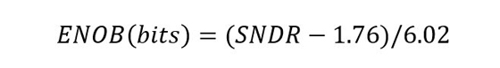
where SNDR is the ratio of the captured signal power to the aggregate power of both noise and distortion.
For example, if an ADC operates with 1 dB of headroom below full scale (FS) and achieves an SNDR of 50 dB, the ENOB will be approximately 8 bits. Note that the SNDR can be referenced to FS using dBFS. ADCs suffer from higher distortion levels when the input signal power is near FS, and the measurements made at lower input power do not linearly extrapolate to measurements at higher input powers.
The input analog linear range of ADCs decreases as voltage supply levels decrease. What was possible with a wider linear range at 5 V power supply levels is now severely reduced at 1 V supply levels. This results in lower saturation levels at the analog input buffer, causing higher distortion relative to the noise floor, readily seen as harmonic distortion using single tone inputs, as well as IMD using multi-tone inputs. The laws of physics governing thermal noise, phase noise, and jitter remain unchanged with supply voltage (except for mild differences in 1/ƒ noise), so that the ultimate resolution of ADCs is limited by fundamental physics and device geometry.
Because the ultimate performance measure of interest is proportional to the energy per conversion for a given number of effective quantization levels, one typically looks to Walden’s overall ADC FOM to determine and benchmark its power consumption P for a given sample rate ƒs and ENOB. The FOM is the energy consumption per conversion step expressed in Joules/conv-step and given by

A lower value of Walden’s FOM corresponds to superior performance. A higher-order effect not expressed by Equation (2) is that the power consumption for a given ENOB does not scale linearly with the sample rate but worsens exponentially above certain sampling rates. FOMs for several ADC IP blocks are reported in the academic literature and in the updated ‘Walden’ tables (now the ‘Murmann’ tables from Stanford University),9 (see Figure 1). This FOM plot clearly shows that there is an inflection point for the performance boundary above 100 MHz, where the best FOM levels rise nearly one order of magnitude for each order of magnitude of increasing sampling Nyquist frequency.
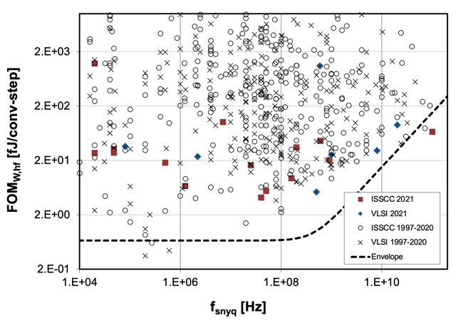
Figure 1 The Walden/Murmann FOM plot versus speed.9
Since the FOM worsens with increasing sample rate and resolution, so does the product’s size, weight, power and cost (SWAP-C). SWAP-C will ultimately determine if the product can be fielded. As a critical component of the product, the ADC will likely be an important factor determining that decision. If the ADC drives too high of a SWAP-C, a more conventional architecture may be prudent, employing lower-frequency ADCs with analog up/down conversion in front of the ADC.
ADC METRICS: JITTER, PHASE NOISE, NOISE FIGURE
The jitter from a clock driving a sample/hold of the ADC is often the most deleterious limiting factor in RF data conversion. The Input Frequency-SNDR trend found by Murmann9 and shown in Figure 2 shows that the highest frequency converters reported so far have achieved a noise floor equivalent of no better than what can be achieved with a clock having a 0.1 picosecond RMS jitter level (dashed line), with an ideal ADC in all other aspects.
The jitter effect depends on the incoming frequency of the signal being sampled, and not the sampling frequency. Errors are induced because the sample-to-sample time fluctuates about the ideal period. The maximum amplitude error is where the incoming signal is at its greatest slope, at the zero crossing. The maximum phase error is where the incoming signal is at its lowest slope, at the positive or negative peaks. Both errors are at their worst at the highest incoming frequency.

Figure 2 The Walden/Murmann aperture error plot.9
A simple and convenient way of understanding jitter error is through the relationship between RMS jitter time relative to the period of an incoming sine wave. The signal-to-jitter noise ratio is thus simply the inverse of the radian fraction of the standard deviation of the jitter, which results in

where ΔtRMS is the standard deviation of the period jitter and ƒin is the incoming signal frequency. Plots of the relationship for an ideal ADC with ΔtRMS values of 1 and 0.1 picosecond RMS are shown in Figure 2 by the solid and dashed lines, respectively.