
The RF-ADC-DFE chain comprises the RF front-end, a variable gain amplifier (VGA), an RF class ADC followed by the DFE. The ADC used in this example is currently available and is capable of directly sampling bandlimited signals up to 8 GHz with a noise density of −151 dBFS/Hz (< −20 dBFS). This performance enables higher-order Nyquist zone conversion. By switching between 6 and 8 GHz sampling clocks, the Nyquist zones can be placed relative to the tuned passbands to cover the desired 4 to 8 GHz operating band. The noise density corresponds to an ADC noise figure of 23 dB and requires the RF front-end and VGA passband gain to be 25 dB to realize a system noise figure of 3 dB at the ADC output. The VGA gain can be adjusted for other combinations of system noise figure and effective RF input full-scale levels.
To achieve a power-efficient front-end design with the required linearity and system noise figure, the two gain stages are designed on a GaN HEMT process. A limiter is not required because of the high power handling of both the GaN amplifiers and tunable RFIC filters, eliminating the loss and linearity degradation of a front-end limiter. Each amplifier uses a cascode topology with degenerative source inductance, an input matching network and complex load and is designed to have flat gain over the 4 to 8 GHz band and be unconditionally stable. The first stage has lower gain than the second, reducing the overall power consumption. To optimize performance, the amplifier operating points can be adjusted to yield power dissipation between 120 and 400 mW. With the nominal bias of 5 V, the bias current in each stage is adjusted for a total power dissipation of 261 mW, where 66 percent is allocated to the first stage to meet the required out-of-band IP1dB.

The RF front-end can be packaged as a surface-mount hybrid module, integrating the two active GaN stages onto a single MMIC die (approximately 2.2 mm x 2.2 mm) that are assembled with two OTFL101 tunable filter RFICs (each 2.6 mm x 1.6 mm in size). The front-end drives the input to the VGA, which provides the single-ended to differential conversion required by the ADC ICs. The VGA driver can be assembled either with the RF front-end or the ADC.
Simulated Performance Results
The design of the RF front-end module was simulated in ADS, employing both the nonlinear GaN models from the process design kit and the behavioral model of the OTFL101. The GaN stages have 11.6 and 14 dB gain, respectively, and the nominal loss of the OTFL101 filter ranges from 5 to 7 dB. This yields an expected gain near 12 dB, confirmed in simulations using “simple tuning,” where all resonators are programmed to the same value.
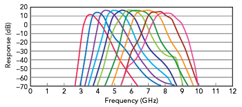
Figure 8 Simulated center frequency tuning of the RF front-end from 3.5 to 8 GHz in 500 MHz steps.
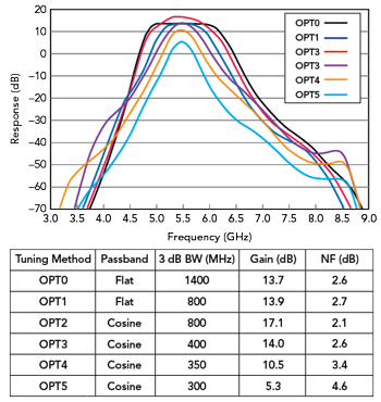
Figure 9 RF front-end tuned to 5.5 GHz showing six simulated bandwidth (BW) and passband states.
Table 3 shows the simulated parameters for the front-end design, using both “simple” and “optimized” tuning, the latter labeled OPT2 V2. The passband gain and relative attenuation at 1 GHz below the center frequency, i.e., fc − 1 GHz, show the optimized case achieves an improvement in all performance parameters: The passband gain increases by ~5 dB, Rstop1 reduces by 29 dB, the noise figure reduces by ~0.5 dB and both the out-of-band input P1dB and input IP3 increase by 3 dB. This indicates improved interstage matching, which increases the power transfer within the signal chain.
Center frequency tuning of the RF front-end is illustrated in Figure 8, which shows the bandpass responses from 3.5 to 8 GHz in 500 MHz steps. The tuning resolution is virtually continuous, given the 5-bit resolution of each of the 10 resonators. At each center frequency, the bandpass characteristics can be adjusted. The best approach is through optimization, where the goals of various desired transfer functions drive adjustment of the bandwidth, gain, passband shape and out-of-band attenuation characteristics.
Figure 9 shows the simulated responses for the front-end design tuned to fc = 5.5 GHz and at several optimized states, labeled OPT0 through OPT5. Their transfer functions are plotted with the corresponding parameters shown in the included table. The plot conveys the capabilities of a chain of two IC filters, each with 10 resonators, to provide various bandwidth, gain and noise figure characteristics. To obtain the simulated results shown in the figure, goals were defined to obtain either a flat passband or cosine shaped response. The flat responses of OPT0 and OPT1 yield two bandwidths with a sharper cut-off. The cosine response, OPT2, produces the highest in-band peak gain and the lowest noise figure, i.e., 2.1 dB. The narrowest passband response, OPT5, has a break point and higher noise figure, i.e., 4.6 dB.
Asymmetrical transfer functions can be used to suppress either a high-side or low-side interferer more aggressively while maintaining the passband sensitivity. An example is shown in Figure 10, for OPT2 V2 in Table 3, which represents the case 2 interference (see Figure 6). The |S21| frequency response (shown at the top) has 17 dB passband gain, dropping to −29 dB gain 1 GHz below the passband center, a relative attenuation of 46 dB. Using a harmonic balance simulation of the entire Rx chain, the output dynamic range versus the interference power for two tones is shown in the bottom plot. The out-of-band input IP3 is +19.7 dBm with transducer gain of 20 dB. The black dashed line represents the received in-band signal of interest, and the blue and red lines are the interference terms at 4 and 5 GHz, respectively. The magenta line shows the in-band third-order IMD term. The simulation results include the 1 dB gain compression of the small in-band signal at an interference power level of +1 dBm. The compression is gradual as the interference power continues to increase above the 1 dB compression point. For single Tx array interference (case 1), a maximum level of +7 dBm results in a 3 dB degradation of the system noise floor, due to gain reduction upstream of the ADC.
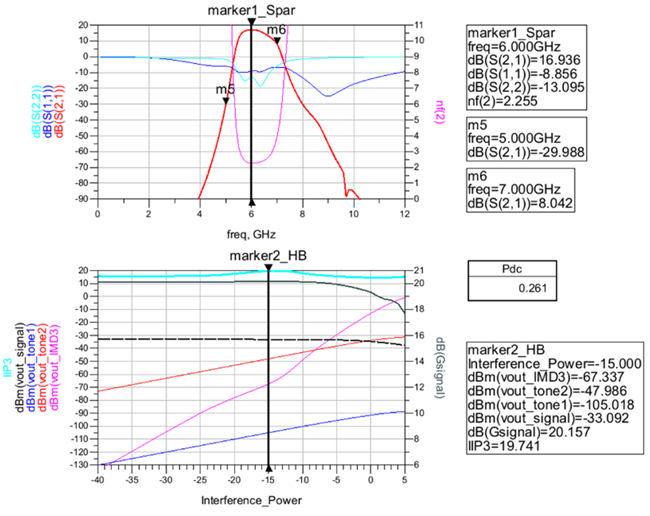
Figure 10 RF front-end asymmetrical tuning response for the OPT2 V2 case in Table 3.

Figure 11 Maximum signal spectral mask for a tuned band with case 1 interference.
Figure 11 illustrates the maximum signal spectral mask for a tuned band supported by this design. For terms within the effective DFE filtering frequency range (shown in green) but outside the passband (yellow), the maximum allowable signal is bounded by the ADC saturation point. For case 1 saturation, the front-end output terms due to interference and distortion close to the passband can be further reduced using the DFE’s more selective decimation filters. Programming of the chain can ensure alignment of both the RF filters and DFE filters. DFE passband equalization will improve the matched filter response and beamforming patterns, addressing phase nonlinearity and element-to-element matching. Adjusting Rx and/or Tx bandwidths and their Δf can be achieved by adjusting the RF front-end and DFE bandwidths between 200 and 800 MHz.
Model Based Optimization
In this article, the RF front-end chain is analyzed within Advanced Design System (ADS), where the foundry’s PDK nonlinear GaN models for the active stages are combined with the ADS version of Otava's behavioral models of the OTFL101 filters. The tuning of the combined chain is optimized based on the predicted S21, S11 and S22 responses within cost functions using a manual random-gradient iterative search method to derive the control states of the 10 resonators employed. Given the accuracy of both the active stage and filter models, the chain model can be used to derive a nominal set of stored states, even without measurement. In keeping with this strategy, the accuracy of the model can be enhanced by training on a set of manufactured units.
To address the variation between units and achieve the highest accuracy, VNA calibration may be used in place of the model. A future optimizer will be developed that complements the behavioral model and eliminates the manual iteration.
SUMMARY
The capabilities and impact of a new class of tunable filters based on SOI RFICs were described, with the aim of increasing the operating bandwidth of the phased array. The combination of linearity, tuning time, small size, tuning degrees of freedom and reliability of the specific RFICs from Otava were analyzed at a device and system level. These devices surpass solutions using switched filter banks, PIN diode2 and MEMS5 switches. RF building blocks such as front-ends, converters and synthesizers can employ the cascade of active/passive stages to realize multiple improvements for wider operational bandwidths.
New capabilities for phased arrays were illustrated with the design of a notional software-defined wideband FDD phased array system, transmitting and receiving simultaneously over C-Band (4 to 8 GHz). The system design example can be reconfigured over the entire band with minimal constraints, while achieving high phased array performance. Notionally, it is possible to support high 5G data rates on both uplinks and downlinks simultaneously from a single node, while adapting to changing electromagnetic environments. This example shows a combination of front-end capabilities and system benefits, addressing such issues as spectral congestion, performance and cost-effective deployment.
References
- R. H. Olsson, K. Bunch, C. Gordon, and N. Zhou, "Creating a universal radio frequency front-end for elemental digital beam formed phased arrays," 2016 IEEE International Symposium on Phased Array Systems and Technology (PAST), 2016, pp. 1-4.
- L. Cifola, et al., "Integrated filtering in reconfigurable planar phased-array antennas with spurious harmonic suppression," 2013 IEEE International Symposium on Phased Array Systems and Technology, 2013, pp. 598-603
- Knowles, “Reduce SWaP, Increase Performance of Phased Arrays with an Innovative Filtering Approach,” Microwave Journal, June 2021, web: www.microwavejournal.com/ext/resources/whitepapers/2021/Jun-21/Knowles_WP_Reduce- SWaP-Increase-Performance-of-Phased-Arrays.pdf.
- G. Qizheng, ”RF Tunable Devices and Subsystems: Methods of Modeling, Analysis, and Applications,” Springer International Publishing Switzerland 2015.
- K. Lee and G. M. Rebeiz, "A miniature 8–16 GHz packaged tunable frequency and bandwidth RF MEMS filter," 2009 IEEE International Symposium on Radio-Frequency Integration Technology (RFIT), 2009, pp. 249-252
- Otava Inc.,"Otava Inc's New IC Portfolio Announcement," Microwave Journal, September 2021, Web: www.microwavejournal.com/articles/36736-otava-incs-new-ic-portfolio-announcement.
- T. Das, “LNA Design Trade-Offs in the Working World,” NXP, December 2010, Web: www.nxp.com/files-static/training_pdf/WBNR_LNA.pdf.
- G. Nikandish, A. Yousefi and M. Kalantari, "A Broadband Multistage LNA With Bandwidth and Linearity Enhancement," in IEEE Microwave and Wireless Components Letters, Vol. 26, No. 10, Oct. 2016, pp. 834-836.
- V. Vanukuru et al., "A 6 GHz 0.92 dB NF Cascode LNA in 180 nm SOI CMOS Technology," IEEE MTT-S International Microwave and RF Conference (IMARC), 2019, pp. 1-4.