
Editor's Note: A condensed version of this article was published in the print edition of the June 2022 Microwave Journal, constrained by the available pages in the issue. This is the author's complete article.
The capabilities and impact of new silicon on insulator (SOI) tunable filter ICs on the design of the RF chains of phased arrays are discussed. These new devices provide an advancement in tunability, small size and high linearity, which supports efficient approaches addressing the challenges of operating with interference overlapping wider operating bandwidths. These devices, with an input IP3 of ~45 dBm and an insertion loss of 5 to 7 dB, can be integrated into the active stages of RF front-ends to suppress both transmit emissions and received interference while also preserving the receiver system noise figure. Within a cascade of stages, higher-order filtering can be achieved. A serial interface to each filter IC controls each resonator independently to realize both its center frequency tuning range and its optimized bandpass characteristics. This functionality helps enable software-defined multifunction phased array systems that are robust relative to interference. To illustrate the advantages of these devices, a wideband, dynamically programmable, frequency-division duplex (FDD) system operating over C-Band (i.e., 4 to 8 GHz), is proposed. An example design of a reconfigurable LNA-to-bits signal chain for digital beamforming is discussed. The example achieves a combination of passband system noise figure and rejection of out-of-band interference by optimizing the tunable filter's variables. To assist system architects in optimizing the benefit of these degrees of freedom, a software tool comprising an accurate behavioral filter model is available.
For RF applications, such as communications and radar, active phased array antennas provide an efficient way to steer and direct the radiated RF energy to achieve the desired effective isotropic radiated power (EIRP) on transmit and the gain over noise temperature (G/T) on receive, which are required for either operating a mobile communications link or detecting mobile targets. To maximize the signal-to-noise and interference ratio (SNIR), the analog, digital or hybrid beamformers can optimally shape the array antenna gain pattern based on measurements of incoming signals, calibration and sounding data to determine the operating channel. Systems employed for military and commercial systems range from smaller arrays with less than a hundred elements and moderate antenna gain to large arrays with thousands of elements, higher gain and pencil beams. However, the performance and benefits of the phased array can be limited by trade-offs within the constituent RF chains, particularly when considering nearby interference.
Among the goals for phased arrays, increasing the operating bandwidth is necessary when increasing their multifunction utility and flexibility. However, widening the bandwidth of the phased array can increase the emissions of unwanted spurious radiation when transmitting, while also exposing the elemental front-ends to higher power interfering transmitters when receiving. Even when this interference is outside the instantaneous band, the limited dynamic range of a "wide open" receive front-end will exhibit blindness or significantly reduced sensitivity.
The array radiating elements are typically designed with low antenna gain and wide beamwidth and are spaced to support the required scan volume for the maximum frequency of operation. The typical spacing, d, is λ/2 for a maximum scan range of ±90 degrees. Therefore, this exposes the elements and their RF chains to both a wide range of angles of arrival and a wide range of interferer frequencies. The RF chains comprise front-end switches, isolators, circulators, power amplifiers (PA), low noise amplifiers (LNA), beamformers, up/down-converters, synthesizers, analog-to-digital converters (ADC), digital-to-analog converters (DAC) and digital front-ends (DFE). Therefore, the ability to reconfigure the properties of the chain to address the effects of emissions and interference on a selected passband within a wider operational band is a desirable capability.1–5
Another important trade-off is the cost effectiveness of the solution. The hardware cost is only one consideration; the service or mission objectives must also be considered. The supporting I/O, local processing, fronthaul and backhaul, platform (or site) size and the required power and thermal design for heat removal are universal factors. A more flexible array architecture with increased operating bandwidth and support for multiple functions is desired for achieving a greater return on investment for commercial systems and improved mission effectiveness for military systems, so long as the key requirements of each function are simultaneously satisfied.1–4
For commercial systems, spectrum licensing led to the prevalence of single band and single function systems. This shifts for military applications, where the size, weight and power (SWaP) limitations of mobile platforms require multifunction capability, software programmability and coverage of more spectrum. The ability to program nodes to address multiple interference scenarios and requirements, while also addressing SWaP and cost, is desirable for military systems and will also benefit commercial systems.

WIDEBAND TUNABLE IC FILTERS

Figure 1 Measured responses of the three tunable SOI RFIC filters.
To fill this need for spectral control and agility, miniaturized high linearity and tunable (or switchable) filters have been developed for use with phased array front-ends. This article discusses the architectures that optimize the system performance using a family of three ICs offered by Otava that cover bands between 2.5 and 40 GHz (see Table 1).6 An overlay of the measured nominal transfer functions of the three ICs is shown in Figure 1. The responses shown reflect “simple tuning,” where all resonators are set to the same control value. With the RFICs flip chip mounted on test boards and the losses of the input and output lines de-embedded, the filter insertion losses are between 5 and 7 dB over a 3:1 center frequency tuning range.
Employing SOI technology with thick copper metal and a high isolation substrate reduces the loss compared to RFICs fabricated with bulk silicon processes. The SOI RFIC’s linearity, power handling and tuning range support flexible operation within active signal chains, avoiding both varactor nonlinearity and the size limitations of switched filter banks. Programming is enabled through a three-wire serial control, where each resonator has 5-bit tuning resolution, enabling center frequency, bandwidth and reflection coefficient tuning. Less than 1 μs is required for configuring the filter characteristics. Power consumption for the CMOS control interface for these otherwise passive devices is under 50 μW.
One way to operate these RFIC filters is through “simple” tuning, where all resonators are programmed to the same value. Beyond this method, the tuning degrees of freedom enable innovative approaches to optimize the performance, given specific interference frequencies, to increase rejection and/or adjust for specific input and output amplifier impedances within the RF chain. To assist system architects explore these capabilities, a companion “wideband” behavioral model has been developed. The model is available at the Otava website and is implemented as a MATLAB APP with graphical interface. Its accuracy has been verified in predicting filter passband amplitude and phase, in addition to sideband skirts down to attenuation levels of −40 dB for both simple and optimized states. Choosing the state to use is best explored using an optimizer, which will be offered in the future.
IMPACT OF TUNABLE FILTERS ON PHASED ARRAY ARCHITECTURES
To assess the impact of these wideband tunable filters, the following requirements should be considered: linearity, sensitivity, operating bandwidth, tuning agility, control of passband gain, interference rejection, element-to-element tracking and array packaging density. The potential locations for filter placement within a phased array front-end are shown in Figure 2. The ideal concept is the “filter first” front-end, either in the common leg (position A) or in the separate transmit (Tx) and receive (Rx) paths (position B). The “filter first” option requires filters with ultra-low loss and high power handling; unfortunately, current technologies for wideband tunable filters do not support the required loss, linearity, power handling and size.
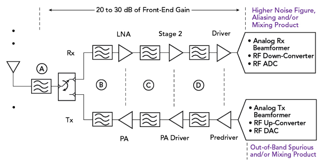
Figure 2 Possible filter placement in a phased array.
An alternative is using a low gain PA output stage and a low gain LNA input stage, both combined with a moderate loss tunable filter at location C. Since additional gain stages are required, adding filters at location D enables a higher-order cascaded filter response, improving performance. The SOI filter ICs shown in Table 1 have the size, insertion loss and linearity to meet the Tx and Rx requirements of this alternative.
For the Tx path, the filters at locations C and D ensure transceiver impairments do not produce spurious out-of-band signals in linear PAs. Amplified out-of-band noise is also suppressed. Given the high linearity of the filters, the high input power needed for low gain PAs (e.g., 20 dBm rms input) will produce spectral regrowth well below that of the PA output stage. The resulting broadband output spectrum amplified by the PA is protected from spillover radiation, a critical requirement for FDD systems.
In the Rx path, distributing the filters downstream in locations C and D reduces the amplification of out-of-band interference. Normally, an Rx chain employs multiple LNA stages to achieve 20 to 30 dB of gain, which is required to minimize the effect of the high noise figure of the downstream components, such as beamformers, mixers and ADCs. Without filtering, the out-of-band interference would be amplified by each active stage. This can be referred to as a “filter last” topology, which requires high LNA power. Another alternative is referred to as a “filter first” topology, which reduces the required LNA power, but at the expense of severely degrading system noise figure due to the loss of the tunable filter.
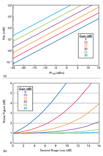
Figure 3 Effect of LNA gain on front-end power consumption (a) and noise figure (b), assuming an LNA with 1 dB noise figure and 15 percent efficiency at the P1dB operating point.
Figure 3 illustrates two of the Rx design trade-offs, analyzing an LNA first stage followed by a lossy or noisy component such as a filter. Figure 3(a) plots the power consumption required versus the IP1dB, assuming the LNA has 15 percent efficiency (see addendum on LNA efficiency for the rationale supporting this assumption).7, 8, 9 Figure 3(b) plots the cascaded noise figure versus the loss of the second component, assuming the LNA has 1 dB noise figure. In both graphs, the performance is shown for gain levels from 5 to 30 dB.