
To operate with 0 dBm input interference, the power dissipation varies from 25 mW to 6.7 W, over the 5 to 30 dB gain levels. A “filter last” approach emphasizes the lowest noise figure with high gain (i.e., greater than 25 dB) at the expense of DC power: greater than 2 W is required to maintain the dynamic range. A more optimum choice employs the “distributed filter” chain, where a first stage gain of 10 to 15 dB is sufficient to achieve a noise figure less than 2 dB, assuming a loss of 6 to 10 dB for each filter. The power required to achieve 0 dBm interference reduces by a factor of ~9x for this “distributed filter” case compared to the “filter last” case and achieves better noise figure than the “filter first” case.
The +45 dBm input IP3 of the tunable IC filters enables a high 30 to 35 dBm input IP3 limit at the input of the Rx chain, which is above the expected input IP3 limit of the preceeding active stage. After this first stage of gain and filtering, the power consumption required downstream to maintain linearity is relaxed for any out-of-band spurious. With this architecture, more of the power is allocated to the first stage to increase the combined out-of-band IP1dB and IP3, while meeting the required in-band gain and noise figure. By distributing the filters between multiple moderate gain LNA and amplifier stages, the effective filter order is increased while reducing the overall power consumption required.
Beyond adding a bandpass filter, system performance can be further improved by optimizing the filter transfer function for various special interference conditions, such as a low or high side interferer. Embedded sensing or frequency planning can provide the knowledge needed for the current RF environment. To determine the preliminary control conditions for lookup, an accurate measurement-driven model is used to predict the response within an integrated chain. These preliminary control states can be updated using vector network analyzer (VNA) measurements of assembled receive chains prior to array integration.
Otava’s SOI RFIC filters (see Table 1) support the distributed filter architecture. They are small enough for assembly in low-cost packaging, enabling integration with other components in a size compatible with the phased array λ/2 lattice spacing. For example, the five pole OTLF101 device (2.3 mm x 1.6 mm die size) supports filtering in arrays up to 8 GHz, occupying only 1 percent of the available area per element. For higher frequency arrays, the OTFL201 occupies 6.6 percent of the available area at 24 GHz, and the OTFL301 occupies 18 percent at 40 GHz. Hence, these devices can be integrated into distributed chains with the front-ends of phased arrays over the 2.5 to 40 GHz range.
C-BAND T/R PHASED ARRAY
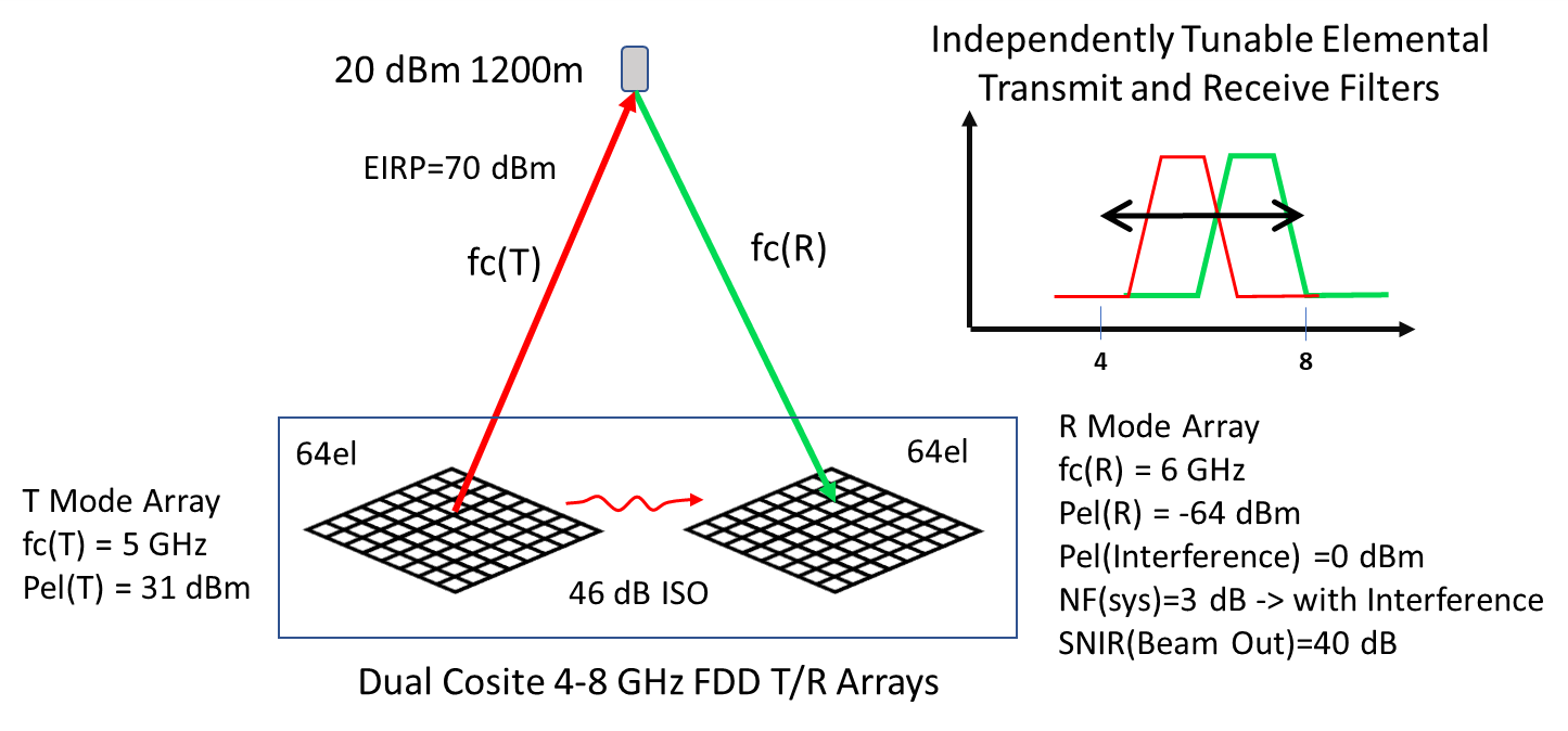
Figure 4 Scenario with dual, colocated FDD capable arrays.
To see the utility of the tunable filter RFICs, consider a system composed of at least two arrays capable of FDD operation over all of C-Band, i.e., 4 to 8 GHz (see Figure 4). While one or more of the arrays transmits, one simultaneously receives, with all the arrays operating at different center frequencies within C-Band. Distributing tunable RFIC filters in the Rx chain (at locations C and D in Figure 2) maintains high sensitivity in the Rx array while high EIRP is generated in the collocated Tx arrays. The Rx RF chain needs to have low in-band noise figure while suppressing high power out-of-band interference from the nearby Tx array.
For this example, assume a wideband, tunable, direct digital beamforming architecture using a currently available higher-order Nyquist RF ADC. By selecting the appropriate ADC sampling rate and RF front-end filter transfer function, the RF chain provides the gain and antialiasing filtering for driving the ADC with multiple in-band and out-of-band conditions. The goal is to maximize the received signal of interest relative to the combined noise, interference and distortion floor at the output of the ADC and, ultimately, the decimation and baseband filtering of the DFE. The primary challenge for the Rx array is maintaining the required in-band sensitivity in the presence of out-of-band interference from the nearby Tx arrays operating within the same 4 to 8 GHz band. Assume the Tx and Rx arrays each use a 200 MHz wide passband and their center frequencies are separated by Δf, where Δf =|fc(T)-fc(R)|. The allowable Tx power is determined by the spatial separation, near-field isolation and frequency separation between the arrays, in addition to the performance of the Rx chain.
Tx and Rx Scenarios
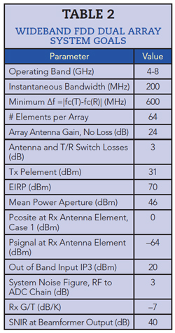
Two cases will be analyzed for the wideband, collocated FDD array systems: the Rx array and one Tx array (case 1) and two Tx arrays (case 2).4 All the arrays have 64 antenna elements with RF front-ends at each element. The notional requirements for the front-end Rx chain for both cases are summarized in Table 2.
For in-band signals, the smaller signal of interest is received over the 200 MHz passband within the operating band. For example, a high data rate downlink uses a 20 dBm EIRP remote transmitter at 1200 m, tuned to a center frequency, fc, of 6 GHz, resulting in a signal power of −64 dBm into the Rx element. A system noise figure of 3 dB provides an effective −88 dBm input noise floor, including ADC noise. The array’s beamforming gain will yield the required output SNR of 40 dB. Notionally, the analog portion of the RF chain is allocated a 2 dB noise figure, driving its output noise floor to a level 5.9 dB above the self-noise of the ADC. The combined noise terms result in the required 3 dB system noise figure, providing 60 dB digitized dynamic range above this floor over the 200 MHz passband. For most RF ADCs, the gain required for this is nominally 25 dB. The ADC’s full-scale output is obtained with a −4 dBm input to the RF chain. An operating full-scale level of −15 dBm — which is 11 dB down from ADC saturation — accounts for any multipath and higher-order modulation received signals. Variable gain in the ADC driver can be employed to modify the digitized dynamic range versus the system noise figure. The SNR at the output of the beamformer is nominally 40 dB for the smaller signal of interest, which is sufficient for high spectral efficiency 5G Gbps data rates.
For the case of single Tx array interference (case 1), the Rx array must operate adjacent to a 64-element array with 31 dBm rms output power per element. This yields a 70 dBm EIRP main beam; with a typical 50 percent antenna efficiency, the total aperture power is 46 dBm. The near-field isolation between the Tx and Rx arrays is a function of the distance between the arrays, the radiator design, loss in any radomes, antenna polarization and any materials between the arrays used for deflection or absorption. While the details of antenna isolation are beyond the scope of this article, an average effective isolation of 46 dB, required for a 0 dBm interference level, is a realistic assumption.
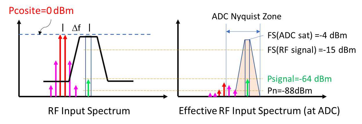
Figure 5 Case 1 RF input spectrum (a) and effective input spectrum at the ADC (b).
From Table 2, the Rx chain must remain linear up to an input P1dB of 0 dBm while suppressing out-of-band interference below the ADC noise floor (see Figure 5). The input from the antenna element is shown in Figure 5(a), and the input equivalent spectrum at the ADC in 5(b). Keeping the passband clear of overlapping interference terms and third- and fifth-order intermodulation distortion is enabled by keeping the T/R frequency separation, Δf, greater than 600 MHz. The figure shows the wide Nyquist zone of the RF class ADC, where the residual filtered terms and aliased terms adjacent to the 200 MHz wide passband can be rejected by digital filtering following the ADC. The exact frequency allocation within C-Band is flexible because 70 percent of the operating band is available. A tighter Δf separation, i.e., greater than 400 MHz, is possible with the input IP5 specified more stringently, which would extend the availability to 80 percent of the operating band.
For the case of two Tx arrays (case 2), the two-tone out-of-band requirement must limit Rx chain degradation from signals from both Tx arrays. The out-of-band input IP3 will depend on the three frequencies selected relative to the filter characteristics (see Figure 6).5 For this analysis, assume the Rx array operates at fc(R1) = 6 GHz, and the Tx arrays operate at fc(T1) = 5.4 GHz and fc(T2) = 4.8 GHz, producing intermodulation distortion (IMD) within the receiver front-end at 6 GHz. To limit SNIR degradation at the beamformer output, an out-of-band input IP3 must be determined. For a 0 dBm two-tone input interference level, a 44 dBm input IP3 for the full chain is required to match the thermal noise floor power. This far exceeds the typical levels of phased array input IP3. For the worst case frequency plans, consider an out-of-band interference two-tone power level of −15 dBm and a very high out-of-band input IP3 of +20 dBm. This results in an input equivalent power of −85 dBm, which is 3 dB above the noise floor. This out-of-band input IP3 can be applied to more complicated interference scenarios, such as widely spread transmitters with unequal power within the operating band.
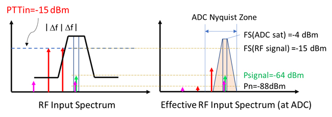
Figure 6 Case 2 RF input spectrum (a) and effective input spectrum at the ADC (b).
FRONT-END DESIGN AND MODELING
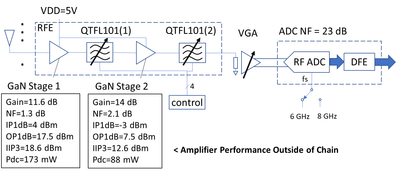
Figure 7 Rx signal chain: RF front-end with GaN MMIC and SOI tunable filters, VGA, ADC and DFE.
The most critical component of the wideband dual T/R array described in the previous section is its high dynamic range RF front-end, which protects the downstream electronics. While this applies to all receivers and beamformers, we focus on interfacing the front-end to a Nyquist ADC with DFE and digital beamforming (DBF) chain, presenting a specific design that meets the challenging front-end and full chain requirements (see Figure 7).