
Other mmWave metastructures can be fabricated that enable amplitude and phase manipulation, near-field interactions and even nonlinear behavior depending on the design and materials involved. A main advantage of mmWave metastructures is the enhanced degrees of freedom and more compact dimensions that can result from periodic, unit cell or fractal metastructure design methods.
Manufacturing process precision is intrinsically significant with 2D and 3D mmWave metastructures, as they require feature sizes on the order of fractions of a wavelength and tolerances of a few percent of the minimum structure size; otherwise, they would operate less efficiently, or even fail to function as intended. This is a particular challenge with dielectrics, as there are limited manufacturing processes that can produce ceramic and glass structures with such small dimensions, conformally and with tight tolerances.1-5 Furthermore, to achieve other performance goals, these metastructures must be constructed of materials with extremely low dielectric losses (low loss tangents), which rules out many polymers and other materials.
Composite materials can be produced with the desired behaviors and assembled through additive manufacturing approaches. There are few additive manufacturing processes, however, that are compatible with complex dielectric composite materials capable of producing relatively large dielectric structures, on the order of centimeters, with high-resolution features on the order of tens of microns.6 There are some promising new composite materials and fabrication approaches that use innovative manufacturing methods to produce structures on such scales that may be useful well into the mmWave frequency range.7
INTEGRATION CHALLENGES
To benefit from a dielectric metastructure it must be designed as a key feature of an AAS or as an enhancement add-on. Either way, the design and fabrication must generally be customized. This is because virtually every physical dimension of the dielectric metastructure must be designed for a specific function. Unlike a radome, which is designed primarily for the protection of a radar/communication antenna, but does not necessarily benefit its function, a dielectric metastructure is a key component designed to critically change the behavior of the electric fields within or radiated/received by the mmWave system.8,9
Integration of a dielectric metastructure, in most cases, requires full electromagnetic (EM) simulation and optimization of the entire mmWave system to fully determine the end-design. This is due to the impact of design integration and fabrication of the integrated assembly on the radiation and electric field behavior within a device and from its antenna structure. This type of simulation is computationally expensive for mmWave structures of any size or complexity, as the mesh refinement and resolution required to achieve accurate simulation results is quite sophisticated. Optimization of a dielectric metastructure may require a substantial amount of time for iterative simulation refinement. It is also likely necessary to characterize the behavior of the lens feed system for a dielectric lens antenna, or the placement and fixture tolerances within the assembly housing.10,11
Manufacturing dielectric metastructures for integration with mmWave systems using traditional layered, cast/molded or CNC subtractive manufacturing approaches may also incur significant expenses for the development of tooling, dies and molds. Consequently, there is a tradeoff between the time and resources spent on design optimization and manufacturing optimization, both of which have their own expense considerations, risks and unknowns. It is therefore desirable to have access to flexible manufacturing methods that can maintain tight tolerances. This is achievable with recently developed dielectric materials and digital light processing (DLP) 3D printing technology.12
DIELECTRIC RESINS & 3D PRINTING
Additive manufacturing technologies have revolutionized many industries, have created new ones and have enabled the fabrication of materials in 3D shapes that were previously impractical to manufacture in all but prototype quantities. This is true for RF dielectric structures as well. Until recently, however, there has been a gap in pseudo-scalable additive manufacturing processes that can yield structures out of low loss RF materials with adequate resolution to perform well at mmWave frequencies.
Traditionally, mmWave dielectrics have been manufactured by layering sheets, forming in molds, extruding to a linear shape or machining to shape from bulk dielectric materials. With additive manufacturing, dielectric structures can now be made in 3D layers with many more degrees of freedom and design flexibility. Additive manufacturing methods, however, come with their considerations.
For example, with fused filament fabrication (FFF), a thermoplastic is forced through a narrow nozzle, similar to an extruding process. The diameter of the nozzle, heating element design, speed of the nozzle translation and thermoplastic behavior dictate quality, repeatability and other manufacturing considerations. One important aspect of FFF is that the diameter of the nozzle heavily influences the final part resolution, but the diameter is also a key determinant in how long a part takes to be deposited (often measured in millimeters per second). For mmWave scale resolutions and surface finish, geometric requirements may necessitate the use of either much smaller diameter nozzles (0.1 mm), precision machining or other post-processing.
With liquid vat photopolymerization methods, such as stereolithography (SLA) and DLP, reaching mmWave scale resolutions is less challenging. Depending on the size of the printer, it is possible to process several parts on a single build plate with the potential for much greater repeatability and finer resolution. With DLP, repeatability and resolution of the developed layers are enhanced with the use of a projector as opposed to a laser in SLA or a nozzle in FFF, which are limited as the patterning with these methods is performed over a point path. A major drawback to vat photopolymerization printing (SLA or DLP) methods has been the lack of available photopolymer resins that exhibit a combination of desirable dielectric constant and low loss tangent, along with low moisture absorption.
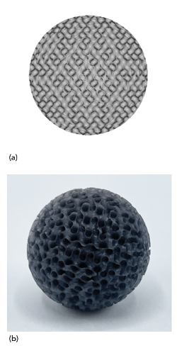
Figure 2 Spherical dielectric GRIN lens model (a) and 3D-printed spherical GRIN lens fabricated with Rogers Corporation Radix 2.8dk printable polymer dielectric using a Fortify Flux Core DLP 3D printer (b).
An example of these dynamics can be found in the fabrication of dielectric metamaterial lenses, such as the mmWave Luneburg-style GRIN lens. A GRIN lens can be fed by switched antennas for beam steering, can enhance a phased-array antenna or otherwise act as a dielectric antenna for a variety of use cases. It can be made by designing air gaps within the structure to effectively reduce the overall dielectric constant within a region using cubic, Kelvin, octet or gyroid unit cell geometries. The design must ensure that the structure is both mechanically stable while providing the effective permittivity range needed to yield dielectric lens properties within a desired volume. In some cases, this may result in feature sizes as small as a fraction of a millimeter (required for mmWave operation) with some low effective permittivity regions requiring very thin and high aspect ratio connecting structures.
LUNEBERG STYLE GRIN LENS DEMO
A DLP projection-based manufacturing method using a photopolymer resin with a suitable dielectric constant and low loss tangent combined with a refined structural design can produce a Luneburg-style GRIN dielectric lens that operates to V- and even W-Band frequencies. The lens is composed of gyroid structural elements that enable fine dielectric gradients while maintaining high structural integrity. Putting these concepts to the test, a joint effort by Fortify and Rogers Corporation has produced a GRIN dielectric lens designed to enhance the directivity and gain of a directional antenna pointed at its center (see Figure 2).
In this case, a coaxial to waveguide adapter (WR12) is used to feed the spherical GRIN lens fabricated with a Rogers photopolymer resin material using Fortify’s advanced 3D printing technology to ensure tolerances are met and to enable the advanced structural design.
The approximately 24 mm diameter E-Band lens is fabricated with wall thicknesses as small as 200 microns (see Figure 2b). The lens is tested using standard methods within a Rohde & Schwarz antenna test chamber with foam gasket fixturing to measure gain at boresight, as well as peak gain at any angle, and efficiency versus frequency.
The 3D printed dielectric lens exhibits a relatively flat gain of between 20 and 22 dBi at boresight from 60 to 85 GHz (see Figure 3a). The average gain of the lens antenna is relatively constant throughout the entire band. Gain fluctuations at boresight likely result and/or are exacerbated due to calibration errors within the setup or slight variations in peak gain angle.
The efficiency data plotted in Figure 3b includes the interconnect loss from coaxial cables, male/female coaxial adapters and the coaxial to waveguide adapter. Additional losses from the test setup are not included. It is expected that the lens antenna efficiency would improve if these losses were included. Additionally, the peak gain trends slightly upward at higher frequencies, which can be attributed to the increased aperture size relative to frequency.
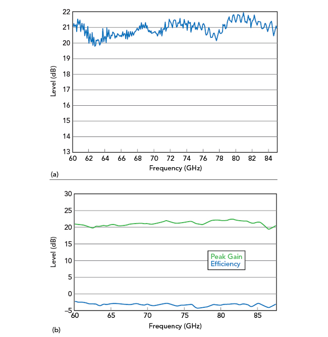
Figure 3 3D-printed, Luneburg-style lens measured gain at boresight (a) and peak gain and efficiency vs. frequency at any angle for the complete dielectric lens antenna (b).
CONCLUSION
The ability to fabricate complex 3D dielectric structures with the necessary accuracy and precision to achieve adequate performance at mmWave frequencies has historically been limited. The need for advance mmWave dielectrics has driven recent advances in electromagnetic metastructure design and materials development. These advancements have resulted in a 3D printable photopolymer resin and 3D DLP printing technology with performance characteristics that have enabled the fabrication of a high gain V- and W-Band dielectric lens antenna prototype.
References
- 1. F. Kamutzki, S. Schneider, J. Barowski, A. Gurlo and D. A.H. Hanaor, “Silicate Dielectric Ceramics for Millimeter Wave Applications,” Journal of the European Ceramic Society, Vol. 41, No. 7, 2021, pp. 3879–3894.
- 2. T. Sebastian, Dielectric Materials for Wireless Communication, Elsevier, 2008.
- 3. Edited by I. Brener, S. Liu, I. Staude, J. Valentine and C. Holloway, Dielectric Metamaterials - Fundamentals, Designs, and Applications, First Edition, 2019.
- 4. E. Semouchkina, Dielectric Metamaterials and Metasurfaces in Transformation Optics and Photonics, First Edition, Elsevier, 2021.
- 5. X. Zhao, G. Duan, A. Li, C. Chen and X. Zhang, “Integrating Microsystems with Metamaterials Towards Metadevices,” Microsystems & Nanoengineering, Vol. 5, No. 5, January 2019.
- 6. “3D Printed Dielectric Lenses Increase Antenna Gain and Widen Beam Scanning Angle,” Fortify, Web: http://get.3dfortify.com/rf-white-paper/.
- 7. Rogers Corporation, “New Material Innovations Guide for 3D Printing High Performance RF Components,” Microwave Journal, eBook, December 2021, Web: https://www.microwavejournal.com/articles/37318-new-material-innovations-guide-for-3d-printing-high-performance-rf-components.
- 8. M. K. Saleem, M. Xie, M. Alkanhal and M. Saadi, “Effect of Dielectric Materials on Integrated Lens Antenna for Millimeter Wave Applications,” Microwave and Optical Technology Letters, Vol. 61, No. 7, April 2019.
- 9. D. C. Mooradd, A. J. Fenn and P. T. Hurst, “Modeling and Validation of a mm-Wave Shaped Dielectric Lens Antenna,” International Applied Computational Electromagnetics Society Symposium, March 2018.
- 10. C. A. Fernandes, J. R. Costa, E. B. Lima and M. G. Silveirinha, “Review of 20 Years of Research on Microwave and Millimeter-wave Lenses at Instituto de Telecomunicações,” IEEE Antennas and Propagation Magazine, Vol. 57, No. 1, February 2015, pp. 249–268.
- 11. F. Ansarudin,T. Abd Rahman, Y. Yamada, N. H. Abd Rahman and K. Kamardin, “Multi Beam Dielectric Lens Antenna for 5G Base Station,” Sensors, Vol. 20, No. 20, October 2020.
- 12. K. Bi, Q. Wang, J. Xu, L. Chen, C. Lan and M. Lei, “All-Dielectric Metamaterial Fabrication Techniques,” Advanced Optical Materials, Vol. 9, No. 1, November 2020.