
COMPRESSION MEASUREMENTS
The 1 dB compression point (P1dB) at the output of a PA defines the boundary between linear and nonlinear behavior. This is the input power where the small-signal gain of the PA is reduced by 1 dB. As the input power increases, the PA becomes increasingly nonlinear and produces significant harmonic distortion and intermodulation products.
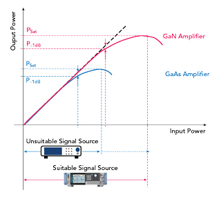
Figure 7 Input power range required for GaAs and GaN PAs.
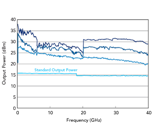
Figure 8 Output power options of the R&S SMA100B signal generator.
GaN PAs have higher saturated output power capability than GaAs PAs. Assuming the same gain, the GaN PA will require higher input power to reach P1dB and the maximum or saturated output power, designated Psat (see Figure 7). For measuring the P1dB and Psat of a PA, the signal source must have suitable output power. Addressing this need, Rohde & Schwarz designed the R&S SMA100B to have four output power options (see Figure 8). From 20 GHz to approximately 38 GHz, the R&S SMA100B provides more than 30 dBm—compared to the 16 dBm available from traditional signal sources. Higher output power from the signal source may eliminate the need for an external amplifier at the output of the source to drive the PA into compression.
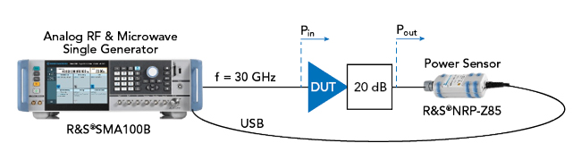
Figure 9 Test setup for measuring 1 dB compression (P1dB) and saturated (Psat) power.
To illustrate this, Figure 9 shows a typical test setup for measuring P1dB and Psat. The power sensor measures the PA output power and feeds back the measurement result to the signal generator via USB, where it can be graphically displayed on the signal generator’s display. The 20 dB attenuator after the PA ensures the power sensor is not overdriven. The DUT is a GaN PA covering 27 to 41 GHz with Psat = 33 dBm and 16 dB gain. The input power (Pin) is swept from -25 to +25 dBm at a carrier frequency of 30 GHz. Figure 10 shows the Pin versus Pout measurements of the PA using a suitable signal source, the yellow trace reflecting the output power and the green trace the linear gain. The y axis accounts for the 20 dB attenuator following the PA. Figure 10a shows a P1dB measurement of 30.2 dBm, and Figure 10b shows a Psat of 33.0 dBm. To measure the Psat of the GaN PA requires Pin = ∼25 dBm at 30 GHz, which is more power than the capability of many signal sources (see Figure 11). Using a signal source with lower output power, P1dB and Psat cannot be measured directly without an additional amplifier. Figure 11 shows 30.0 dBm maximum output power from the PA, which reflects the shortfall of the signal source rather than the performance of the PA.
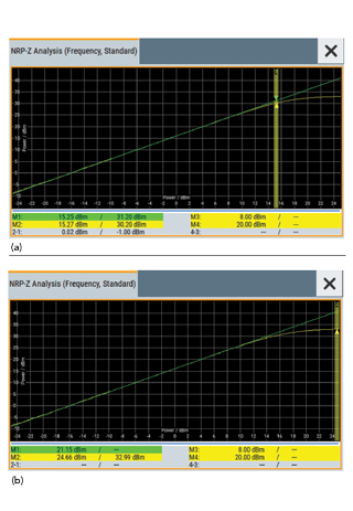
Figure 10 P1dB (a) and Psat (b) measurements using the suitable signal source.
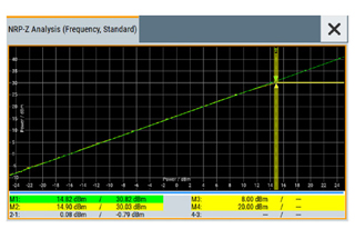
Figure 11 P1dB measurement using the unsuitable signal source.
These measurements show that using a signal source with sufficient output power simplifies the test setup, enabling higher power P1dB and Psat measurements without requiring an external amplifier that could introduce measurement errors.
SSB PN MEASUREMENTS
Analog and digital circuits rely on pure clock signals. Typical clock signal performance indicators are PN, jitter, wideband noise and spurs. Similarly, a low PN signal source is needed for measuring DUT performance. The residual PN of the DUT determines the PN added by the DUT to the PN of its input signal. Phase-locked loops in high speed digital applications require an input signal with excellent PN performance, i.e., negligible compared to the residual PN of the DUT.
How can designers ensure the signal source meets the requirements for SSB PN? First, the requirements for the DUT should be defined. Next, the data sheet of the signal source should be reviewed to determine whether the SSB PN performance meets the requirements with enough margin to minimize the contribution from the signal source. We illustrate this with measurements showing how suitable and unsuitable signal sources affect SSB PN measurements. The R&S SMA100B is used as the suitable source, with the option for a maximum SSB PN of -128 dBc/Hz at 10 kHz offset from a 10 GHz carrier and typically providing -132 dBc/Hz. The unsuitable signal source has a specified SSB PN performance of -115 dBc/Hz at 10 kHz offset from a 10 GHz carrier. Although usable for many applications, this signal source may no longer be sufficient to for testing current generation analog-to-digital (ADC) and digital-to-analog (DAC) converters.
In this example, the DUT was a test board with a DAC. The best way to measure the residual SSB PN of the DAC is to generate a sinusoidal signal at its output, where the digital input is I = Q = 1. The DAC used here has a digital signal processing unit with a digital up-converter, enabling the digital input data to be resampled and shifted in frequency. The numerically-controlled oscillator of the DAC was set to fout = fsample /9, with fsample = 9 GHz, so the DAC output signal was a 1 GHz sine wave.
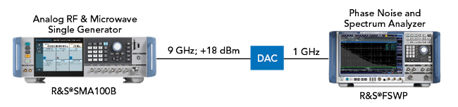
Figure 12 Test setup for measuring the SSB PN.
As with the previous measurements, the setup comprised the two signal sources and the DUT; an R&S FSWP was used to measure the SSB PN (see Figure 12). The SSB PN was measured with the suitable signal source, with and without the DAC, and the unsuitable signal source, with and without the DAC. Figure 13 shows the SSB PN measurements of both signal sources at 9 GHz with +18 dBm output power and “downscaled” to 1 GHz by subtracting 20log(9 GHz/1 GHz) in dB. Downscaling is necessary to compare the SSB PN performance of the signal sources and the DAC.
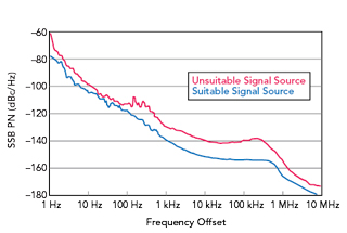
Figure 13 Comparing the SSB PN measurements using the two signal sources.
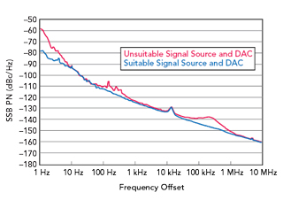
Figure 14 Comparing the SSB PN performance of the DAC using the two signal sources.
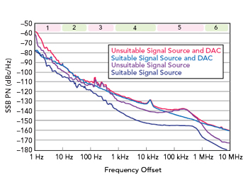
Figure 15 1 GHz SSB PN comparisons.
Comparing the SSB PN performance of the DAC with the two signal sources, the difference in specific frequency ranges was high (see Figure 14), with the lower curve the SSB PN performance of the DAC measured with the lower PN source. The SSB PN measurement using the unsuitable signal source adds significant contributions to the DAC’s residual SSB PN. To show where the poorer signal source influences the SSB PN measurement, the offset frequency range was split into six bands (see Figure 15). In ranges 2, 4 and 6, the measured DAC SSB PN performance was nearly same with both signal sources, as the SSB PN of the unsuitable signal source was better than that of the DAC. In frequency ranges 1, 3 and 5, the SSB PN of the unsuitable signal source was worse than the DAC’s performance, so the SSB PN measurement reflects the performance of the unsuitable signal source, not the DAC.
These measurements show the importance of using a low PN signal source. To ensure accurate measurements, follow this process:
1. Measure the SSB PN performance of the signal source using the same frequency and power level as will be used for the DAC measurement. In this example, the DAC output frequency was 1 GHz, so the DAC clock input signal of 9 GHz was divided by 9 in the DAC.
2. Calculate the SSB PN performance of the signal source at 1 GHz to compare it with the DAC output frequency of 1 GHz: SSB PN (1 GHz) = SSB PN (9 GHz) − 20log (9 GHz/1 GHz) in dB.
3. Ensure sufficient margin between the DAC measurement and the calculated SSB PN of the signal source.
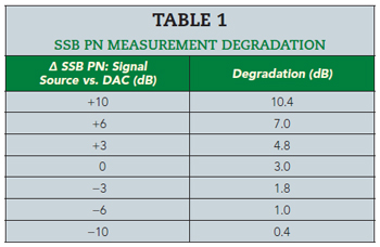
Table 1 shows how the SSB PN of the signal source will degrade the measurement of the DAC’s performance. The table shows if the SSB PN of the signal source is 10 dB better at a certain offset frequency than the DAC’s performance, the measurement will be degraded by 0.4 dB.
The instrument used to measure the SSB PN is another potential source of measurement error. Although not assessed in this article, a phase noise analyzer with low SSB PN should be used for these measurements to minimize any degradation.
SUMMARY
This article has examined how the harmonics, output power and SSB PN performance of the signal source can degrade measurement accuracy, often without the user realizing the unwanted effects. In each example, the performance of two signal sources was measured, showing the effect on a PA or DAC measurement. Guidelines for harmonics and SSN PN were provided to quantify the impact of the signal source, enabling users to determine the appropriate signal source requirements to achieve the desired accuracy for the application.