
IoT modules are often defined by their small form factors and ability to transmit sensor data to a centralized hub via a wireless connection. While the radio modulation scheme and IoT protocol can vary, most IoT devices fall below the 6 GHz band. For these IoT applications there is a need for small planar antenna structures implemented on a common PCB platform where connection to the microcontroller unit (MCU) and processing unit of the node is accomplished often via a push-on miniaturized coaxial interface. This article examines the various PCB antenna implementations and their design considerations, with an additional discussion around the packaging and placement of IoT nodes and how this can impact their connectivity.
THE MYRIAD OF IoT DEVICE CONSIDERATIONS
Power and size constraints often cause IoT nodes to run off either a simple coin-cell battery or small form factor energy storage device for an extended period (on the order of years). To accomplish this, a low energy-consuming protocol must be employed with different “classes” and/or “power modes” to enable different levels of energy savings. For instance, a LoRa device has various current modes (i.e., transmit, receive, synthesizer, standby, idle and sleep) to enable the sensor node to extend its operating lifetime, enabling minimal maintenance and repair.
The frequency of uplink/downlinks are also particularly relevant for battery savings—scheduled uplinks and downlinks enable less latency, a higher throughput and greater reliability while asynchronous, ad-hoc transmissions can extend range and battery life at the expense of data rate and payload size.
Extensive energy harvesting techniques have often been leveraged for IoT devices, allowing for a relatively unlimited battery life without human intervention. This, however, does increase node cost and complexity.
Regardless of the industry, IoT devices often leverage cellular, Bluetooth and Wi-Fi protocols as they are prolific and therefore easy to integrate and scale with the native system for monitoring and control. Often, multi-protocol IoT platforms incorporate a more niche IoT protocol (e.g., ZigBee, LoRa, Sigfox, etc.) as well as a Bluetooth low energy (BLE), Wi-Fi or cellular module to incorporate the benefits of both. A device that leverages Wi-Fi can more readily connect to the cloud, allowing for control/configuration as well as firmware upgrades from any remote location.
A node that includes both BLE and a sub-GHz low-power wide-area network solutions can provide Bluetooth beacons for a real-time location system while also remotely controlling a simple mechanism such as industrial lighting from a distant location. Still, there are the major considerations of test and certification that come with Bluetooth and cellular devices. Both protocols require extensive testing and proof before they can come with the required “stamp of approval” for release.
WHY CARE ABOUT THE ANTENNA?
In the massive landscape of IoT sensor technologies, protocols, vendor-specific SoCs and development boards, often overlooked is the antenna, link budget and integrity of the wireless link between nodes. Typically defined by an omni-directional radiation pattern with a specific vertical/horizontal beamwidth, most IoT devices use either a whip, PCB or chip antenna. In cases where specific fringe devices must be connected, directional antennas (e.g. Yagi) can be used to extend range. Each antenna type has its respective benefits and considerations.
PCB antennas are particularly effective due to their balance between gain and size. The characteristic low profile of the PCB antenna allows it to be readily configured within a case as opposed to jutting out like the classic whip antenna. Unlike the chip antenna, PCB antennas can operate over relatively large bandwidths with relatively high gain. A trace antenna can even be embedded into a system-level board during the manufacturing process allowing for a smaller device form factor.
Beyond real estate considerations, antenna design and placement can come with significant link integrity considerations—radiation quality can be directly impacted by neighboring electronic components, metallic enclosure hardware and of course, environmental interference. Factors such as transmit/receive antenna gain, free space path loss at a specific carrier frequency, loss of the antenna feed, transmitter and receiver losses and miscellaneous environmental losses must be considered when attempting to expand the link budget. Regardless of the environment, however, radiation pattern, gain, VSWR and bandwidth are parameters preliminarily evaluated in the first steps of development and optimization of a wireless connection.
UNDERSTANDING COMMON TRACE ANTENNA DESIGNS
PCB antenna structures can be monopole, dipole, slot, patch and printed inverted-F (PIFA). There is a plethora of books, application notes and blogs dedicated solely to the design of each with extensive equations; the following is intended as an overview of the trace patterns used and their practical considerations.
Dipole and Monopole Antennas
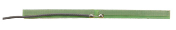
Figure 1 This 2.4 GHz dipole trace antenna achieves 2 dBi gain.
A dipole antenna comprises two quarter wavelength (λ/4) long metallic strips with a total electrical length requirement of a half wavelength (λ/2) at the carrier frequency for maximum response (see Figure 1). Much of the trace antenna literature is devoted to the design of antennas in the 2.4 GHz ISM band due to the use of conventional protocols such as Bluetooth and Wi-Fi. At 2.4 GHz, the length of the dipole antenna is approximately 6 cm, which could be unreasonably large for some applications. The omni-directional radiation pattern has a concentration of electromagnetic energy perpendicular to its length (z-axis) with a null in the middle (along the z-axis). This often requires it to be placed in a vertical orientation for maximum horizontal coverage—a serious consideration for designers intending to use a dipole (or monopole) antenna in an IoT device.
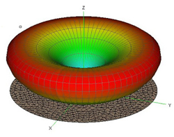
Figure 2 Monopole antenna pattern showing ground plane effects.
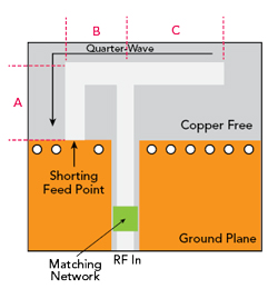
Figure 3 PIFA board layout.
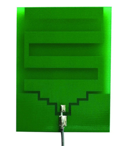
Figure 4 This 800/900 MHz MIFA antenna achieves 2 dBi gain.
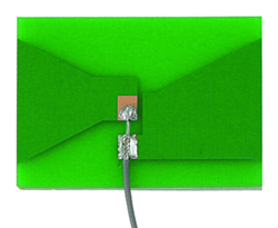
Figure 5 Planar conical dipole or bow tie antenna.
Figure 6 Dipole antennas using bent conductive elements to save space.
Figure 7 Dual-band 2.4/5 GHz omnidirectional planar dipole antennas.
The addition of a ground plane eliminates one arm of the dipole, resulting in a structure that consists of a singular quarter wavelength conductive element with the ground plane acting as the other quarter wavelength arm. Analogous to a mirror, the ground plane generates a “virtual image” of the radiation pattern that is equal (same current flow direction and phase) to the one generated by the conductive strip. For the ground plane to function optimally, it must be considerably larger than a half wavelength. A finite ground plane results in edge diffraction of the radiated wave causing electromagnetic energy to move radially outward from the edge and leak behind the ground plane.1
Ideally, with a perceptually infinite ground plane, the gain of a quarter wavelength monopole antenna should be twice that of a half wavelength dipole due to reflection from the ground plane radiating exclusively toward the area above it. This results in a somewhat “lifted” pattern (see Figure 2). Once again, a null is created along the length (z-axis) of the conductive quarter wavelength element revealing an ideal vertical orientation.
Bent Monopole Antennas
Bent monopole variants such as the L-shaped (or tilted whip and inverted L), planar inverted-F (PIFA) and meandered inverted-F (MIFA) structures leverage the same ground plane and conductive arm methodology with varying patterns of the conductive arm. The bend in the trace allows for a more compact size as well as decreasing the null in the radiation pattern. In these designs, however, the antenna trace typically must not run too close to ground as this can cause the antenna to act as a transmission line without any radiation.2
Of these variants, the PIFA is the most common due to its small PCB area and wide bandwidth performance. As shown in Figure 3, it has a fold in the main resonant line that introduces a capacitance canceled out by the shorting feed point at the end of line. Impedance matching with the antenna feed is obtained by adjusting the lengths of A, B and C, where the dimensions of A and C contribute to the quarter wavelength element and B is adjusted for an impedance match. An external matching network can also be included for additional tuning.
The MIFA antenna (see Figure 4) is like a helical or spiral antenna, as it increases the total length and accomplishes resonance with varying orientations of trace/wire compressions. In a MIFA, horizontal and vertical lines form multiple turns. Like the PIFA, tuning is accomplished by adjusting the geometry within the meandered line. This effectively reduces the size of the antenna. However, it often comes with tradeoffs such as reducing gain and therefore shortening range, relying more on tuning and therefore exhibiting a narrower bandwidth and increasing sensitivity to interference from external sources as well as native electrical components on the board.
Dipole Antenna Variants
Printed dipole antennas face a major size disadvantage. At low frequencies this is especially relevant; here, a monopole antenna element has the advantage that it can potentially be placed on a corner of the board with the ground plane serving both as the RF ground plane/return path of the antenna and ground for the native electrical components of the IoT module. As the operating frequency increases, however, this becomes less of a concern. Moreover, like bent monopole antenna structures, different dipole patterns can be employed to increase bandwidth and decrease size.
Tapering the dipole arms is a known bandwidth enhancing technique. For example, the planar conical dipole antenna, also known as a bow tie antenna (see Figure 5), behaves as a uniformly tapered transmission line. When an RF signal is applied across the feed, currents flow radially outward and form an enclosing magnetic field. However, currents are abruptly terminated at the edge of the bow tie causing more reflections and a narrower bandwidth than its 3D, biconical counterpart. Still, a relatively constant impedance and gain can be achieved over a massive frequency range relative to other dipole antennas. The antenna in Figure 5 exhibits a high gain (4.5 dBi) over a large bandwidth (4.9 to 5.9 GHz).
Along the same line of reasoning found in bent monopole quarter wavelength antennas, smaller form factors can be achieved by meandering the conductive arms of the dipole elements (see Figure 6). As previously mentioned, this optimizes the Q but can decrease overall bandwidth and efficiency. Therefore, the use of self-resonant space-saving techniques such as the spiraling or meandering of the conductive arms comes with tradeoffs that must be considered for the application.
GENERAL PLANAR ANTENNA CONSIDERATIONS
Board Layout
There are some general design principles to consider to achieve the most benefit from the low profile form factor and potential space savings. For monopole antennas, sufficient ground planes are critical; a good quality/large ground plane enables an improved VSWR and a closer correlation with theoretical antenna behavior. For planar antennas integrated onto the module board, there is a keep out area around the antenna that requires the board to be free of copper traces or ground fill. In multi-layer designs, vias along the edge of the keep out area are necessary to connect ground planes.
Antenna tuning, or the minor adjustment in trace dimensions or length of the conductive arms, must be done within the enclosure and not in free space, as the enclosure and environment in which it functions affects its radiation performance. Moreover, any changes in layout often lead to changes in antenna performance and therefore must be tested.
Antennas with thicker trace widths often have broader bandwidths, as can be seen with structures such as the conical dipole antenna. Beyond trace thickness and length of the conductive elements, the relative permittivity (εR) and thickness of the substrate material (e.g., FR4, flexible PCB (FPCB) and Teflon) also affect antenna performance.
Impedance Matching
Impedance mismatches cause unnecessary reflections and signal loss, so a lumped element matching network such as a pi- or T-match at the antenna feed allows for maximum power transfer. More complex matching networks enable tuning with series and shunt inductive and variable capacitive elements such as MEMS switches. Other variations include single-stub or multiple-stub tuners that provide broader bandwidth at the expense of space. These structures reduce the effects of external factors such as changes in orientation as well as the effects of obstacles and objects that are near the antenna that can cause signal degradation while matching transmission and reception bands necessary for the application.
Dipole antennas have found use in a wide array of applications due to their ability to accommodate a MIMO implementation in LTE/5G systems with relatively straightforward multi-band, dual-polarization designs (see Figure 7). An integrated microstrip balun is often used to match the impedance of the antenna and transmission line. A differentially fed planar dipole antenna is also used with an integrated Marchand balun to provide a balanced transition between the antenna and its feed network. Dual-polarized planar dipole antennas have been realized through the formation of two identical elements of varying orientations while exhibiting low cross polarization.3
Enclosures
IoT devices and sensor nodes often come in ruggedized enclosures to prevent damage from environmental elements such as wind, precipitation, UV damage, humidity and salt water. Enclosures that are NEMA-rated and/or IP-rated can be used: however, these do not consider the effects that the various parts will have on antenna radiation patterns. Even a molded plastic enclosure can cause RF losses and should therefore be tested and characterized prior to manufacture. A polycarbonate casing will exhibit different signal loss characteristics than a thermoplastic casing and, of course, a stainless steel enclosure. Metallic components such as pads, pins, tracks and ground planes can cause the antenna to lose efficiency, gain and bandwidth while metallic casing components such as brackets, padlock, screws/studs and even an external pole mounting kit will cause signal degradation.
In some applications, the casing itself is used to adjust the antenna radiation pattern. For example, altering a dipole antenna radiation pattern can be accomplished via a director or reflector strip. A director strip adjusts radiation elements within the antenna to change its frequency response while the reflector strip, or metal part of the antenna casing, adjusts the antenna radiation pattern to fit an area of coverage and potentially support ceiling/wall installations. When leveraging a commercial off-the-shelf (COTS ) PCB antenna, it is important to verify its performance both inside and outside of its enclosure to ensure that the structure does not negatively affect desired performance.
Certifications
IoT device certifications are an essential part of the design process from prototype to production. This is particularly true for Bluetooth and cellular devices. For example, the GSMA defines the over-the-air (OTA) testing of IoT devices using 3GPP communications (e.g., NB-IoT, LTE-M and CAT1/CATbis) in its TS.51 report.4 Tests and performance requirements are defined for total radiated power and total radiated sensitivity. These parameters evaluate antenna performance where poor OTA performance would result in a high block error rate, as well as potential access failure. When using the unlicensed spectrum however, the most critical design consideration is typically conforming to FCC EIRP regulations.
CONCLUSION
PCB/trace antennas suit a wide range of applications with narrow single-band and multi-band options. The size and shape of the antenna can be reduced using common bending/meandering techniques however, this comes with an array of efficiency and sensitivity considerations.
A higher gain antenna will loosen the constraints on the link budget, wider traces often correspond to a larger bandwidth. Still, these come at the cost of size, and in the world of IoT the miniaturization of sensor nodes, ease of installation and scalability are serious considerations.
A COTS antenna comes with the benefits of a proven antenna structure with verified performance, but this does not ensure that the antenna will function within an enclosure of choice.
The basic structures of a simple monopole (e.g., PIFA and inverted L) and bent dipole are popular choices. Nevertheless, these antennas are only a few of the many possibilities depending upon the carrier frequency, operating bandwidth, polarization, size and cost.
References
- E. Holzman, “Essentials of RF and Microwave Grounding,” Artech House, Norwood, MA, 2006.
- AN2731: Compact Planar Antennas for 2.4 GHz Communication, NXP Semiconductor, Rev. 4, November 2020.
- Iswandi, M. N. Z. Akbar, A. K. D. Jaya and E. S. Rahayu, “Modification of Multi Band Printed Dipole Antenna for Indoor Base Station of LTE Systems,” 10th International Conference on Information Technology and Electrical Engineering, July 2018, pp. 551–555.
- OTA Testing of IoT Device, GSMA, V. 2.0 Feb 2021, www.gsma.com/newsroom/wp-content/uploads//TS.51-v2.0.pdf.