
A K-Band stacked-field-effect transistor (FET) power amplifier (PA) with high linearity and superior temperature stability is implemented in 90 nm trap-rich high-resistance SOI-CMOS technology. The PA adopts a two-stacked-FET architecture and low loss coplanar waveguide (CPW) matching networks to improve the RF output power and power-added efficiency (PAE). The PA with an area of 0.63 mm2 demonstrates a peak power gain of 14.6 dB at 23.5 GHz, a saturated output power of 14.2 dBm with a 3 dB bandwidth of 6 GHz and a peak PAE of 23.5 percent. The measured output third intercept point (OIP3) of 28.4 dBm represents a high linearity feature for 5G communication applications. The RF characteristics at different temperatures from -40°C to 125°C demonstrate superior temperature stability for automotive radar applications.
K-Band MMICs for 24 GHz automotive radar and 5G communication applications have drawn widespread attention in recent years. Typical K-Band MMICs were typically realized in expensive SiGe BiCMOS and GaAs pHEMT technologies.1-3 Thanks to continuously improved cut-off frequencies of highly scaled CMOS transistors, advanced MMICs based on CMOS technologies can now meet the cost and integration requirements for these high frequency electronic systems.4-7 K-Band PAs fabricated in bulk silicon CMOS technologies, however, encounter severe performance degradation in high temperature environments, such as near car engines.5
K-Band PA linearity for 5G applications is an important property that is hard to achieve in bulk CMOS, however.6 SOI-CMOS technologies utilized in the production of ICs for high temperature applications and can provide higher cut-off frequencies, better linearity and lower loss passive components than bulk CMOS. Consequently, SOI-CMOS technology has become a cost-effective choice for high performance K-Band applications.
In this article, a K-Band stacked-FET PA with high linearity and superior temperature stability is implemented in 90 nm trap-rich high-resistance SOI-CMOS technology. The cut-off frequency of the SOI nMOSFET is higher than 90 GHz. A common source architecture is used in the drive stage and a two-stacked-FET architecture is chosen for the output stage. Small and large-signal measurements verify linearity, and temperature stability is measured from -40°C to 125°C.
PA DESIGN
Stacked-FET Architecture
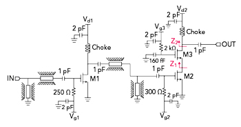
Figure 1 Single-ended, two-stage PA architecture.
The PA in this work is designed for high linearity and high temperature stability based on a trap-rich SOI-CMOS process. Figure 1 shows the full schematic of the single-ended two-stage architecture, including a drive stage and an output stage. Each MOSFET operates Class A.
Generally, the output power of a PA fabricated in highly scaled Si CMOS technology is limited mainly by its low breakdown voltage; however, the stacked-FET configuration distributes the swing voltage equally in each MOSFET. Theoretically, a k-stacked-FET architecture can tolerate k times the breakdown voltage, improving output power and reliability. The most important aspect of the design is the load impedance seen at the drain for each MOSFET. Consequently, a small capacitor is connected to the gate of the common-gate MOSFET M3 in parallel to tune the load impedance seen at the drain of M2 and control the drain-source swing voltage of M2 and M3.
Design of CPW Lines and Inductors
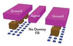
Figure 2 CPW line without dummy fill under the signal line.
The inductors and CPW line structures usually encounter high substrate-induced losses due to the relatively high substrate conductivity in the bulk CMOS process. In this work, a trap-rich high-resistance substrate provides low dielectric losses and low cross talk in the PA blocks. The input and inter-stage matching network are designed using CPW lines. High-quality factor multi-turn RF-choke inductors are made with two layers of thick copper interconnects. They may also be realized using CPW, however, a long CPW line leads to a larger chip area.
In a sub-100 nm CMOS process, the requirements for RFIC design are stringent. Small floating metallization called dummy fill is used to adjust the metal density and suppress the thickness variation of interconnects; however, dummy fill can influence the electrical performance of transmission lines and inductors used in microwave and mmWave circuits.8 Consequently, the use of dummy fills should be considered carefully. As shown in Figure 2, dummy fills under CPW lines are removed to minimize the impact to microwave passive components.
Output Stage MOSFET Sizes and PA Stability
The load-line method is used and the optimum load impedance (Ropt) is calculated for high output power. Tradeoffs are considered carefully in this design to determine output power, Ropt and output stage MOSFET size. Generally, a larger MOSFET can provide higher output power and smaller Ropt; however, a large size MOSFET is usually designed with gate fingers in parallel, which can form an extremely small input impedance and make it difficult to design a wideband input matching network. In the design of this PA, the size of the output stage MOSFET is 3.125 μm × 32 fingers to minimize the effect of gate series resistance. According to the simulation results, the largest drain-source voltage for M2 and M3 is around 2.4 V. Maximum drain current is almost 80 mA, and the knee voltage for M2 and M3 is about 0.3 V. For a single MOSFET,

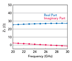
Figure 3 Simulated Z1 vs. frequency.
Pout is the output power estimated empirically. For a two-stacked-FET architecture, an additional 3 dB power gain can double the output power to 16.2 dBm, which is a suitable value for point-to-point wireless communication permitted by the Federal Communications Commission (FCC). The band from 22 to 29 GHz has also been opened by the FCC for short range radar applications. Large bandwidth versus high output power is needed in this application.
The load impedance (Z2) seen at the drain of M3 is tuned to 2Ropt, which is 52.5 Ω and close to the standard 50 Ω load impedance. Consequently, an output matching network is not required and the circuit area is reduced. The impedance (Z1) seen at the drain of M2 is tuned to Ropt, which is 26.25 Ω. The simulated real and imaginary parts of Z1 (see Figure 3) show the impedance optimized to approximately 26 Ω from 20 to 30 GHz with a 160 fF capacitor connected to the gate of M3.
Small resistors connected to the gates of M1 and M2 are used to supply bias voltages and enhance circuit stability. A 2 pF MIM decoupling capacitor is connected to each biasing pad in parallel to minimize the influence of bonding wires, which also aids stability. The Rollett stability factor, K, of the PA is simulated and is greater than 1 for all frequencies between DC and 30 GHz. Transient simulation confirms that each output stage MOSFET has the same swing voltage at high output power, especially at high drive level.
MEASURED RESULTS
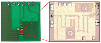
Figure 4 MMIC PA and characterization board.
Figure 4 shows the printed circuit board (PCB) for chip measurements and a microphotograph of the PA. The area of the entire chip is 0.9 × 0.7 mm including pads. The PCB provides DC bias for the PA with 1 and 10 μF capacitors added in parallel. Vdd of the drive stage is 1.2 V and Vdd of the output stage is 2.4 V. Infinity ground-signal-ground microprobes are used for on-chip measurement. No signs of oscillation at any drive level or wire bond inductance are observed.