
The temperature stability of the RF output power level has become especially important for different handheld wireless communication systems. For GSM mobile handsets, an analog closed-loop power control, incorporated in the transmitter power amplifier (PA) chain, allows the main parameters of the PA to be stabilized over the ambient temperature range required by industry standards. This can be done due to a fixed level of the input power driving the GSM PA. However, the power level stabilization for the driver stages is still an important issue. This can be done as well, at the expense of some efficiency degradation of the PA. All existing CDMA mobile transmitters (cellular, PCS, UMTS, cdma2000) do not have a direct closed-loop power control of the RF PA, resulting in the need of a careful design, taking into account the temperature stability of the parameters as one of the main features. Gain variations of 3 to 5 dB over the operating temperature range are usual in existing CDMA PA with fixed drive signal levels and fixed bias and control voltages.
For WLAN applications, Intersil (now Conexant) utilizes a closed-loop power control for the 802.11b/g frequency band (2.4 to 2.5 GHz). Here, a power detector samples the transmitter output power and the base band chip adjusts the power with a certain tolerance. This approach works well to compensate for the temperature variations of an entire transmitter chain as well as component production tolerances. However, the component tolerances in the output chain between the power detector and the antenna connector, as well as the accuracy of the detector characteristics using standard components and existing PCB structures from different vendors, are still creating output power variations of at least ±1 dB at temperatures between +25° and +85°C.
ATMEL utilizes an open-loop control circuit approach for its 802.11b WLAN system PA. It uses a thermistor to stabilize the PA parameters. However, the changes in output power still exceed 2 to 3 dB over the +25° to +85°C temperature range. Not just the transmitter front-end shows variations of output power over temperature because of the output PA used in the circuit. The small-signal RFIC transceiver driving the final PA itself has at least a 1 dB power drop between +25° and +85°C. The test results also depend on the platform used because of the different heat sinking. In the meantime, the PA is the most current consuming device in the transmitter chain and its behaviour plays a crucial role in the output power temperature dependence. An important fact is that the RF PA, used for wireless applications, is a nonlinear device operating under large-signal conditions, resulting in variations of its spectral characteristics over temperature as well (not only gain and power). Because the current need of the industry is low power consumption, the PA vendors are supplying amplifiers with high efficiency. In this case, the spectrum efficiency (ACPR) and digital signal quality (EVM) may be degraded even if one can stabilize the output power by driving the PA input with a closed loop like Intersil. On another side, a large temperature variation requires a larger dynamic range of the transceiver, creating stability problems and increased current consumption (to have a large enough margin to compensate for gain variation). Moreover, the temperature calibration is a time and cost consuming process during mass production. Therefore, one has to stabilize the power output with small variations of the transmitter gain, retaining a reasonable spectrum purity and digital signal quality (such as EVM). This article presents a possible low cost solution that could be used in different wireless communication transmitters using a “linear” PA.
Methods Used for Stabilization
The main parameters of RF CDMA power amplifiers, which are influenced by ambient temperature variations, are power gain and linearity expressed in adjacent channel power ratio (ACPR) for adjacent and alternate channels. The gain and ACPR (at the rated output power) variations over temperature are caused by many factors, such as the transistor current gain (?) change with temperature, leading to an alteration of the I-V characteristics, the fr and fmax values change with the particular current setting of the transistor used and the heat dissipation ability from the active cells of the PA to the heat sink, etc.1 Moreover, all of these variations are dependent on the initial (quiescent) bias conditions of the PA. The situation becomes more complicated with the requirements for a small quiescent current when the idle bias operating point requires class AB or near to class B operation of the PA. The wide range of operating current and self-biasing effects present more challenges with parameter variations.
Consider GaAs HBT power amplifiers that are mostly used today in the wireless industry. The collector current of an HBT, biased by a voltage source through the base resistor RB, can be expressed as2
where
IS = saturation current
VBE and IB = base emitter voltage and base current, respectively
T0 and T = ambient and junction temperature, respectively
? = thermo-electric feedback coefficient (a ª 1.2 to 1.3 mV/°C for GaAs HBT)
The base current can be represented as
where
IP = hole current component
C = hole and electron current
ratio at the emitter junction at ?E = 0
?E = effective difference in energy barrier seen by electrons and holes
? = current gain
At the collector-emitter voltage VCE applied to the transistor, the junction temperature can be expressed in the form
![]()
where
Rth = thermal resistance of the HBT from the junction to the heat sink
From Equations 1 and 2, one obtains

For reference, Figure 1 shows the simulation plot (Equation 4) of the collector current change in percent, versus the base voltage change in mV for the reasonably high current levels used in a mobile GaAs HBT-based PA at a fixed temperature (the base ballast resistance has been chosen to be minimum as well). Although the process variations and the absolute temperature may change this plot a little, this curve gives a good starting point to evaluate a PA and tune the circuit.
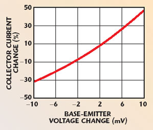
Fig. 1 Typical collector current variation vs. base voltage for HBT transistors.
It is known that stabilizing the power gain and collector current over temperature at different power drive levels results in a stable output power and spectrum purity for digitally modulated standards with non-constant power envelope signals such as QPSK, OFDM, etc.3 From Equation 4, one can see that maintaining a constant base voltage for the transistor results in a very complex temperature dependence of the collector current. Even for a fixed ambient temperature, a positive temperature feedback loop inside the semiconductor hetero-structure results in obvious variations of the I-V characteristics for different base resistances connected for measurements.2 Connecting a “right” base resistance value can cure this problem for a fixed temperature.2 This resistance value, however, is dependent on the absolute temperature and this approach cannot be implemented over a wide temperature range. As well, the thermal resistance variations between the transistor and the heat sink play a great role in the compensation. This base ballast resistance is usually chosen as low as possible to prevent the so-called thermal runaway in HBT structures (both GaAs and SiGe devices4) and protect them from destruction and, at the same time, to maintain the highest possible power gain value. The ? value for the transistors available in industry varies from one vendor to another (within 50 to 300 in most cases) and is dependent on the particular technology process used. Each foundry provides different transistors with different temperature dependence of the current gain.
The common way to stabilize the HBT temperature parameters is the current mirror circuit presented in Figure 2. This circuit allows the collector current to be stabilized over wide temperature variations. R2 is the base ballast resistance. The collector current through L2 is proportional to the current through R1. The simulated collector current change versus temperature for this circuit is shown in Figure 3 for two different reference voltages applied to the Vref pin (2.7 V is often used for high power operation and 1.7 V is often used for low power CDMA PA operation to save current consumption5). It shows that the current mirror circuit can maintain the collector current within ±4 percent for large current operation. However, this variation reaches ±12 percent if one wants to implement the low power operation function as well. By choosing the resistor R1 as an external one, with a positive temperature coefficient of approximately +667 ppm/°C, one supposedly can stabilize the collector current for large-signal operation. At the same time, the small-signal current stability could also be improved. If one chooses the external resistor R1 with a +2019 ppm/°C temperature coefficient for the final small-signal current stabilization, the large-signal current temperature stability becomes worse. Therefore, some trade-off is needed if one has to use the power saving ability. More complicated current mirror and other biasing circuits are available to minimize the gain variations of bipolar transistors over temperature.6
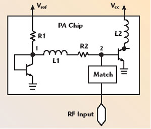
Fig. 2 Current mirror circuit for biasing PA stages.
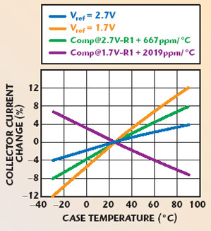
Fig. 3 Current mirror circuit temperature stability.
The entire previous discussion above could be true if the ? of the transistors used in the circuit is independent of temperature. However, even for the InGaP structures, which claim the “lowest” sensitivity of parameters over temperature (compared to the AlGaAs previously widely used in industry), the ? variation over operating temperatures exceeds 40 percent7 for a fixed collector current and is directly transformed into power gain variations. For reference, Figure 4 shows some typical dependences of ? versus temperature for a fixed collector current for InGaP and SiGe HBTs available in the market (the current density has been chosen reasonably high). It is obvious that ? is decreasing at elevated temperatures. The SiGe HBT has a much lower temperature dependence than the GaAs device (this depends on the Si and Ge relative contents in the structure). Sometimes ? has a maximum value at mid-temperatures that is dependent on the particular structure used and current density chosen. RFMD has developed a special molecular beam epitaxy process (MBE) for InGaP HBTs to keep ? almost constant versus temperature. This process is currently used for W-CDMA PAs.7 Careful design of the SiGe HBT profile avoids variation of ? over temperature or even “reverses” its slope.8 Alvarino, et al.7 are also using a closed-loop current control circuit shown in Figure 5. Each transistor stage on the GaAs chip has a control circuit provided by the silicon chip. Both chips are embedded into the same plastic package. Only the precise reference voltage resistor R3 is placed outside the package. The variation of the quiescent current is within 12 percent of the nominal value at room temperature for a 3.4 V bias supply and standard production tolerances.7 Although the quiescent current is tightly controlled, the power gain variation versus temperature between –30° and +85°C reaches 5 dB at the frequency extremes for a maximum rated power of 27.5 dBm for WCDMA operation. Therefore, to stabilize the gain at large-signal operation, one has to fix the large-signal current (for reference, the quiescent current for a PA used in mobile communications can be 5 to 10 times lower than the large-signal current).

Fig. 4 Typical current gain change over temperature for different HBTs.
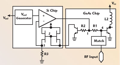
Fig. 5 RFMD CDMA PA closed-loop current control circuit.
Proposed Circuit and Test Results
Usually, all the power amplifiers for wireless communications available in the industry utilize a stable voltage reference provided externally or internally by the low dropout voltage regulator (LDO). This stability requirement is made obvious from the curve of collector current variation as a function of changes in base voltage. Instead of keeping this voltage constant, one has to change it over temperature to keep the gain and output power constant. The question is, what should be this dependence? To evaluate it, the bias mirror circuit (three-stage InGaP HBT PCS-CDMA PA) has been used where the voltage mirrors and each active transistor has been biased directly from the voltage source through the small ballasting resistor R2. All RF matching has been maintained as for standard up-link PCS-CDMA operation with maximum available output power of 28.5 dBm for the particular transistor stage and an ACPR of approximately –50 dBc. Three different size transistor structures (correlated with particular stages) with 250 ?m2, 950 ?m2 and 6750 ?m2 emitter areas have been tested (the current density is approximately 20 kA/cm2). The reference voltage has been adjusted and the base-emitter voltage has been measured over temperature while keeping the collector current constant. The test results for those transistor stages are shown in Figure 6.
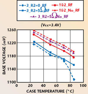
Fig. 6 Base voltage for constant output power and collector current.
The lower blue dashed line represents directly the base-emitter voltage for the largest transistor (marked as no. 3). The blue solid line is the voltage measured through a 5 ? resistance inserted in series with the base of the same transistor. It is obvious that the insertion of the 5 ? resistance is preventing a thermal runaway at temperatures higher than +70°C and it “linearizes” the base voltage curve needed to maintain a constant collector current. The small-size transistors’ stages already have series base ballast resistances on-chip greater than 30 ? and the base voltage versus temperature needed to stabilize the collector current is linear as well. The same behaviour applies for both large-signal operation and idle current. Moreover, it can be seen that all base voltage curves are almost parallel to each other. Therefore, if one can provide a decreasing linear reference voltage dependence over temperature, a stable collector current and output power can be achieved. The same result can be found from Equation 4, using a reasonably large base resistance value. An absolute voltage level is not as important as the temperature slope. Of course, it should not be forgotten to put a large enough value of a ballasting resistance and not to supply the base directly from a voltage source to prevent a thermal runaway. In this case, a simple resistive divider circuit may be used for all stages with biasing from a single voltage reference source.
To verify the proposed principle of output power stabilization over temperature, the circuit in Figure 7 has been used. A high precision adjustable LDO, with ±1 percent tolerance, has been used to provide a stable reference voltage to all three transistor stages of the amplifier. In the feedback circuit, a resistive divider with one thermistor has been used to provide a decreasing, “almost” linear voltage at the appropriate level (this approach is similar to the one used by MAXIM to drive LCD displays9). The resistors R1, R2 and Rt play the main role; R3, R4 are used just to shift the absolute voltage to the level needed for each particular stage. All three base chains are connected to the point 1 of the circuit through the ballast resistors R5. The LDO used had a 1.235 V nominal reference voltage. The negative temperature coefficient (NTC) thermistor type 0402 has been used as a control element (±5 percent nominal tolerance and B = 3650K ±3 percent). A linear slope of 120 to 130 mV is needed to provide temperature stability of the collector current. This is accomplished by R1 in parallel with Rt and R2. The silicon LDO chip and the GaAs PA chip have been mounted on the same laminate PCB (a modular approach has been used). Rt has been positioned on the same PCB between the silicon and GaAs chips.
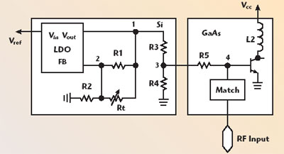
Fig. 7 Test circuit used for current stabilization over temperature.
The compensation voltages are shown in Figure 8. The red solid line represents the voltage needed at point 3. The three dashed lines below represent the LDO reference voltage data provided by vendor. The upper red dashed line is the theoretical line at point 1 calculated for the reference voltage provided by vendor. The blue solid line is the real measured data at point 1. The brown and green lines present the calculated data for production tolerance margins that may be useful for yield evaluation.
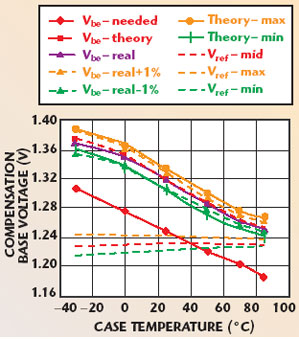
Fig. 8 Base control voltage test and simulation results.
To match the real (blue) line for the point 1 of circuit with the needed (red) line at point 3, the resistive divider R3, R4 is used. It is obvious that the real line can match the needed one with fairly good tolerance (just low temperature and high temperature have some discrepancy). The main intention was to keep the large-signal collector current constant at the 28.5 dBm level for PCS-CDMA operation (up-link mobile) at room temperature. Figure 9 shows the test results of the current changes over temperature for different VCC voltages applied to the PA. It can be seen that the large-signal operation current (for 28.5 dBm at VCC = 3.4 V) has the minimum variations through temperature (+5 to –1 percent), although the quiescent current variations are maximum for this case. Changing the VCC voltage level also results in wider margins of the operating current variations.
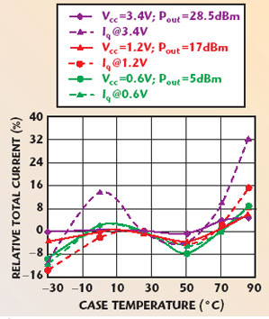
Fig. 9 Current test results for the proposed circuit.
The large-signal gain variation is less than 2 dB for VCC = 3.4 V (see Figure 10). Mainly, this gain variation is caused by the discrepancy between the needed and real base voltage curve at low temperatures. For temperatures from +25° to +85°C, the gain varies by less than 0.3 dB. At lower vcc voltages, the gain varies by 2 and 3.5 dB, respectively. However, this is not as important as for VCC = 3.4 V, since the driving circuit has already “enough” gain margin. The large-signal ACPR over temperature, shown in Figure 11, exceeds the standard specification. The room and extreme temperature test results, for gain and ACPR versus output power level (with changing input drive signal level), are shown in Figures 12 and 13, respectively. It is obvious that, at low signal levels, the gain variation is larger than for maximum rated power. At the same time, the ACPR margin is well below the standard requirements. The intermediate temperature dependence of the parameters is presented in Figures 14 and 15, showing quite well the stability of the parameters.

Fig. 10 Gain test results for the proposed circuit.

Fig. 11 ACPR test results for the proposed circuit.
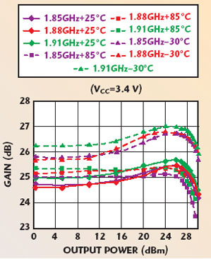
Fig. 12 Gain test results for the proposed circuit at room and extreme temperatures.
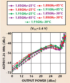
Fig. 13 ACPR test results for the proposed circuit for room and extreme temperatures.
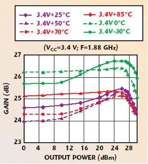
Fig. 14 Gain test results for the proposed circuit for intermediate temperatures.

Fig. 15 ACPR test results for the proposed circuit at intermediate temperatures.
The low VCC voltage operation gain and ACPR over temperature shown in Figures 16 and 17 show the suitability of implementing this thermo-compensating circuit with DC-DC VCC control to substantially increase the efficiency of PA at low and mid power levels.10
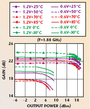
Fig. 16 Low Vcc voltage gain test results for the proposed circuit.
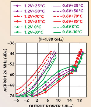
Fig. 17 Low Vcc voltage ACPR test results for the proposed circuit.
Circuits Proposed for Gain Versus Temperature Stabilization
The proposed power stabilization principle is suitable not only for PA designers but for systems designers as well, with some preliminary knowledge of the PA internal structure.
Consider the circuit in Figure 18. First, one has to evaluate the point 1 voltage dependence required for the current stabilization. A particular LDO should then be chosen with a known temperature dependence of its reference voltage (not only its tolerance) so it results in different final output parameters. It is obvious that different LDO part numbers have a different shape of the reference voltage over temperature even for the same tolerance at room temperature. It should be noted that a smooth shape of the reference voltage versus temperature (increasing or decreasing with temperature such as shown in Figure 19) is preferred to “linearize” the base voltage control curve. Any “bending” or “kneeing” at mid-temperatures has to be avoided. The ATMEL solution, mentioned previously and seen by the author, has this problem with an incorrectly chosen LDO. It is also important to choose the correct tolerance for the other resistors used in a circuit (such as 0.1 to 1.0 percent) and their temperature coefficients as well (±50 ppm/°C is a good choice). In this case, the circuit designed may be suitable for high volume production. By changing the resistor values in the circuit, one can create a different temperature shape of the voltage needed (not only linear). Placing the thermistor, LDO and PA close to each other on a common PCB will allow compensating for the temperature variations of the whole transmitter circuit. It is important to know that one does not need to follow an exact value of temperature. One just needs to shrink the possible range of those variations. Special care should be taken during the assembling process. Thermistors “do not like” overheating during a soldering procedure. The vendors usually provide data sheets with some tolerances that include the soldering procedure margins. Following these assembly procedures is a must.
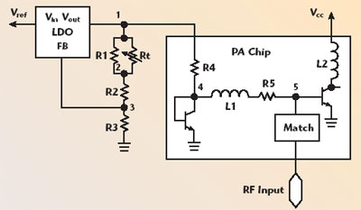
Fig. 18 Thermo-compensating circuit that may be implemented with any PA.
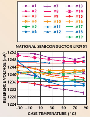
Fig. 19 Several LDO test results over temperature.
An example of the circuit design procedure is described below:
Consider the thermo-compensating circuit shown previously. Let us suppose that the ballast resistance R5 is low and ? = 50. Apply a voltage V1 = 2.8 V to pin1. The voltage at point 4 is approximately +1.25 V at room temperature (for InGaP and AlGaAs HBT). Let the current through resistor R4 be 5 mA. In this case, the resistance R4 value is R4 = (2.8–1.25)/0.005 = 310 ?. The thermo-electric feedback coefficient is chosen as a = 1.2 mV/°C. By that, one needs the voltages of 2.866 and 2.728 V at point 1 at –30° and +85°C, respectively, to stabilize the collector current. The LDO reference voltage is chosen as Vref = 1.175 V. Let it be stable with temperature. Choosing an NTC type of resistor Rt, with a 1 k? nominal value at +25°C and a thermal coefficient B = 3650K, R1 = 750 ?, R2 = 6.8 k?, R3 = 5.227 k? results in a voltage variation at point 1 between 2.733 to 2.862 V at –30 to +85°C, which is very close to what one needs. Some fine-tuning is necessary for real devices for which the test data is available.
For very tight control, a high precision LDO may be used, like the MAXIM part with up to ±0.1 percent tolerance (although their price is higher than for less tolerant ones). For a highly linear voltage control curve, high precision (±0.12 percent) thin film platinum resistance temperature detectors may be used.11 A 5 GHz WLAN PA with a thermo-compensated circuit is shown in Figure 20. The price of these Pt-RTDs is comparable to the NTC ones. As before, let us consider some real situations. The base current drawn through R4 is 2 mA (as in reality). The voltage at point 1 is 2.9 V at +25°C. The point 1 voltage should be 1.188 and 1.318 V at +85° and –30°C, respectively. Consider only the output transistor stage of the PA with ? = 50. For the same LDO, with a 1.175 V reference voltage, the choice of Rt = 1 k? as Pt-RTD, with TCR = 3750 ppm/°C (and ±0.48 percent tolerance), R1 = 7.5 k?, R2 = 4 k?, results in the perfect match needed.
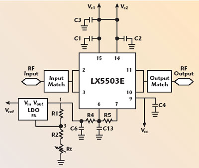
Fig. 20 Example of a highly linear thermo-compensating circuit.
These examples show that the LDO introduction to the circuit elevates the current consumption of the whole circuit by only 0.2 to 0.3 mA. The circuit proposed allows utilizing easily the power shut-down function and the power control function as well. All the speculations above are valid for different types of RF PA used in wireless communications (GaAs, Si, SiGe, bipolar, HBT, MESFET, CMOS, Bi-CMOS, etc.). Only the absolute voltage levels and their shape over temperature are different. The circuit proposed is very flexible and may be used successfully in different portable wireless systems.
Conclusion
The simulation and test data considered in this article, along with the circuits proposed, may be applicable to the existing and future designs for mobile phone and WLAN PAs. Not only the RF PA output power can be stabilized over temperature but the entire transmitter RF chain as well. Certainly, the closed-loop power control approach may be used in addition to the circuits considered (analog-loop or through base band) to eliminate variations of supply voltages and production tolerances as well. By that, one will be aware that the most nonlinear part of the transmitter already has no problems with temperature.
The gain/power stabilization circuit can be implemented as a small size module with one or several adjustable components (resistors) placed externally. The use of this circuit in an entire transmitter chain will replace the LDO currently implemented in many designs (mobile phones, WLAN, etc.) to keep a stable PA control voltage.
References
1. M. Hafizi, W.E. Stanchina, R.A. Metzger, P.A. Macdonald and F. Williams, “Temperature Dependence of DC and RF Characteristics of AlInAs/GaInAs HBTs,” IEEE Transactions on Electron Devices, Vol. 40, No. 9, September 1993, pp. 1583–1587.
2. Y. Zhu, J.K. Twynam, M. Yagura, M. Hasegawa, T. Hasegawa, Y. Eguchi, Y. Amano, E. Suematsu, K. Sakuno, N. Matsumoto, H. Sato and N. Hashizume, “Compensation of Self-heating Effect in DC and Pulse Characteristics of HBTs,” 1999 IEEE MTT-S International Microwave Symposium Digest, pp. 431–434.
3. RF Micro Devices, “A High Gain Power Amplifier with Variable Bias for Multi-mode WCDMA Applications,” Microwave Journal, Vol. 45, No. 2, February 2002, pp. 154–167.
4. P.D. Tseng, L.Y. Zhang, G.B. Gao and M.F. Chang, “A 3 V Monolithic SiGe HBT Power Amplifier for Dual-mode (CDMA/
AMPS) Cellular Handset Applications,” IEEE Journal of Solid-State Circuits, Vol. 35, No. 9, September 2000, pp. 1338–1344.
5. J.A. Roche, R.M. Healy, G. Hau and S.A. Caron, “Adaptive DC Power Management for HBT PAs in CDMA Handsets,” RF Design, February 2002, pp. 42–50.
6. Y. Deval, et al., “1-volt Ratiometric Temperature Stable Current Reference,” 1997 IEEE International Symposium on Circuits and Systems Digest, pp. 1984–1987.
7. K. Alvarino, H. Bui, S. Coryell, S. Egolf, H. Jiang, C. Lazinbat, E.T. Spears, D. Spooner and D.A. Teeter, “Next-generation CDMA2000 1x Power Amplifier Modules,” Applied Microwave & Wireless, pp. 74–84.
8. T. Johansson and W.X. Ni, “Feasibility Study of 25 V SiGe RF Power Transistors for Cellular Base Station Output Amplifiers,” Material Science & Engineering B89, Elsevier, 2002, pp. 88–92.
9. “Using Thermistors in Temperature Tracking Power Supplies,” Maxim Integrated Products, Article A244, September 2001.
10. E.C. Glass, J.H. Huang, J. Staudinger, M. Shields, M.J. Martinez, O.L. Hartin, W. Valentine and E. Lan, “Application of Enhancement Mode FET Technology for Wireless Subscriber Transmit/Receive Circuits,” IEEE Journal of Solid-State Circuits, Vol. 35, No. 9, Sept. 2000, pp. 1276–1284.
11. Syntec Corp., Taiwan, data sheet, 2003.