
FR4 is used as the PCB substrate in the simulation with relative permittivity 4.8 and dielectric loss tangent 0.017. Antenna is designed to operate at 2.4 GHz which is the desired Bluetooth frequency. As can be seen from Figure 9(b), the reflection coefficient of the antenna at 2.4 GHz is -17 dB which validates the design of the antenna.
On a real PCB assembly, there are many components of various materials that can affect the antenna performance. To study the effect of these components, we embed the antenna module on the PCB designed and shown in Figure 3 that holds all electronics circuits. The PCB and its components are simplified to evaluate antenna performance. Figure 10 represents the antenna placed near the Bluetooth IC. Different electromagnetic material properties assigned to the various components on the PCB are shown in Table 2.

Figure 10. Antenna integrated on the PCB.
Table 2. Material properties of components on the PCB.
|
Material Name |
Relative permittivity |
Dielectric Loss tangent |
|
HDPE |
2.3 |
0.0003 |
|
FR4 |
4.8 |
0.017 |
|
LDPE |
2.2 |
0.0003 |
|
PTFE_teflon |
2.08 |
0.0004 |
After the antenna is placed on the PCB, it is observed that the resonant characteristics have changed. The reflection coefficient plot in Figure 11 shows that antenna would suffer significant losses due to mismatch as reflection coefficient around 2.44 GHz has reduced from -17 to -3.95 db. To restore the performance, a matching circuit to the antenna is designed and added. The components of the circuit are shown in Figure 12.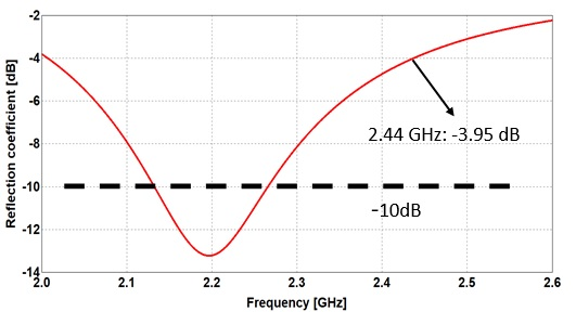
Figure 11. Reflection coefficient after antenna integration on the PCB.

Figure 12. Matching circuit.
Once the matching circuit is added, antenna performance is observed by plotting the reflection coefficient and radiation pattern that displays the values of realized gain as seen in Figure 13. It is observed that the resonance occurs at 2.4 GHz and the value of reflection coefficient at the frequency is much improved. The reflection coefficient at 2.44 GHz is -25 dB. The antenna operates for a bandwidth of 250 MHz around the desired frequency. This means that the received signal will not suffer mismatch losses. The doughnut shaped radiation patterns similar to a dipole antenna’s validates our BT antenna design on the PCB.

Figure 13. Antenna characteristics after adding matching circuit: (a) Reflection coefficient, (b) 3D radiation pattern, (c) 2D radiation pattern.
Antenna Placement inside a Speaker cabinet
Now that we have integrated the antenna on the PCB and checked its performance, it is needed to perform an in-situ analysis where the antenna with the PCB to be placed in its real environment inside a smart speaker cabinet shown in Figure 14. Antenna placement analysis helps in optimizing the location of the antenna inside its actual environment. It also aids in analyzing the overall performance of the product. Simulating such an environment can improve or ease the decision-making process and reduce costs significantly. The other components inside the speaker include metallic heat exchanger, fan for cooling, acoustic port and speaker module. The speaker cabinet chosen is made of balsa wood that has dielectric constant of 1.3. The fan for cooling is made of Teflon. The length and the breadth of the speaker cabinet is 355 and 305 mm while the height is 450 mm.
When selecting the location and orientation to mount the PCB with the antenna, several factors like spacing inside the cabinet, mount support options and thermal efficiency can limit the number of iterations to be simulated. We simulated the performance of the antenna by changing the location and orientation to make a best possible location that considers some practical constraints. The parametric sweep option in Feko is used to automate the simulation process for all possible locations.
Location 1 includes the PCB antenna placed near the back wall of the Bluetooth speaker in such a way that the antenna is facing toward the back side of the speaker as shown in Figure 14 (a). Location 2 and 3 include the PCB mounted on the same back wall, facing inward, but the antenna is located on the top and bottom side respectively as shown in Figure 14 (b) and (c). Location 4 and 5 include the PCB mounted in the free space between the components, facing inward and close to the back wall and the front wall respectively as shown in Figure 14 (d) and (e).
Fig. 14. Antenna placement: (a) Location 1, (b) Location 2, (c) Location 3, (d) Location 4, (e) Location 5.
The reflection coefficients from all other iterations are plotted on the same cartesian graph as shown in Figure 15 to make a decision on the best PCB location. Except for location 1, reflection coefficient is better than -10 dB for all other locations.
Figure 15. Comparison of reflection coefficients: Location 1, 2, 3, 4 and 5.
The 3D radiation patterns of locations 2, 3, 4 and 5 are shown in Figure 16 and respective 2D polar plots for both principal planes are shown in Figure 17.
Figure 16. 3D Radiation patterns: (a) Location 2, (b) Location 3, (c) Location 4, (d) Location 5.

Figure 17. Comparison plot of total realized gain for locations 2, 3, 4 and 5: (a) theta = 90, (b) phi = 0, (c) phi = 90.
As can be seen from the simulations, location 1 can be discarded due to poor reflection coefficient performance. Similarly, for location 4, radiation pattern appears to be focused on one side of the speaker with very low gain values in other directions. For optimal performance, the antenna should have uniform gain in all directions. Locations 2 and 3 are suitable for the placement of the antenna for optimal performance. For further analysis such as coverage and interference we select Location 2 as the best position.
IV. Wireless Coverage and Interference for Smart Products
With the advent of 5G and Internet of Things (IoT), the trend is towards smart household electronics, including speakers. These smart devices operate on several technologies, like Wi-Fi, Bluetooth, LTE, ZigBee, etc. for various applications. Because of the congested spectrum, some of these technologies operate within closely separated frequency bands, leading to interference.11 Especially, the Bluetooth and Wi-Fi co-exist and operate around 2.4 GHz and the interference from Bluetooth affects the Wi-Fi throughput and vice versa. Therefore, it is important to analyze the interference levels through virtual prototyping at the early design stages to avoid costly rework after the final design. The effect of interference from Wi-Fi on the Bluetooth speaker is evaluated inside a multi-story residential building using Altair’s wireless propagation and radio network planning software, WinProp,9 as shown in Figure 18.

Figure 18. Multi-story residential building: (a) Complete house, (b) Cross-sectional view.
For an accurate analysis, the residential building is modelled as a detailed multi-story design with thick walls, flooring, staircase, fireplace, cabinets, doors, windows and roof. The Bluetooth speaker is placed in one corner of the living room while the Wi-Fi router is in the corner of an adjacent room, as shown in Figure 18 (b). The speaker is operating on the latest Bluetooth 5 technology12 while three different Wi-Fi technologies, namely the 802.11b, 802.11n and 802.11ax [13, 14, 15] are considered for the router.
Bluetooth Coverage
The Bluetooth speaker has a near omni coverage along the horizon, as depicted in the previous section. This section describes the RF channel characteristics of the speaker inside the building when operating on the Bluetooth 5 technology. This technology supports a maximum data rate of 3 Mbps for Up Link (UP) and Down Link (DL) through the enhanced data rate transmission mode, while the high speed mode supports 2 Mbps and the long-range modes support 500 Kbps and 125 Kbps in UL and DL. The results from the network analysis, as shown in Figure 19, illustrates that the enhanced data rate transmission mode is serving the entire house except for a small area in the corner on the opposite side of the speaker location. The Bluetooth technology is a packet-based protocol with a master/slave architecture, with one master communicating with up to seven slaves in a piconet. Therefore, for this CDMA based technology, the maximum number of codes available for user on one carrier are seven. Ideally, these codes will be perfectly orthogonal to each other, however, in a real-life environment like a residential building, a reasonable 0.8 orthogonality factor is considered. This results in a maximum achievable DL throughput of 19 MBps, as shown in Figure 19 (b).

(a)

(b)
Figure 19. Bluetooth network parameters: (a) Maximum DL data rate, (b) Maximum achievable throughput in DL.