
For about half a century the suppression effects of bandpass hard limiters on various combinations of signals and interference have attracted widespread interest.1-4 Certain "rules of thumb" have accreted around a variety of theoretical results. The purpose of this article is to revisit issues of interpretation and to indicate the possible role of more sophisticated demodulators in the abatement of suppression. Attention is focused specifically on the effect of the bandpass hard limiter on the input combination of a sinusoidal signal and a powerful constant-envelope interferer. In such a situation the effect most commonly cited3 is the 6 dB suppression of the signal. The first step in comprehending and interpreting this suppression effect is the definition of a bandpass hard limiter within the intended context.

Definitions and Classical 6 dB Suppression
A bandpass hard limiter generally spans a band of radio frequencies whose width is relatively narrow compared with the center frequency (theoretical analyses of the limiter's action often employ the corresponding "narrowband assumption"). The purpose of a bandpass hard limiter is to deliver a constant carrier envelope output when the input envelope fluctuates gradually with respect to the radio frequencies within the passband. The hard limiting effect is generally attained in practice by driving an appropriate radio frequency amplifier into saturation. Theoretical modeling of a limiter, however, may proceed through the alternate route of dividing the limiter input by the envelope of that input to develop a model of the constant-envelope output.
The frequency components of an exemplary elementary signal plus strong interference are illustrated in Figure 1(a) . A signal at carrier frequency f2 = 1 MHz is combined with a strong interferer at f1 = 900 kHz, and the combination of the two is passed through a bandpass hard limiter whose passband (by definition) stops short of any harmonics of the input frequencies. The interferer amplitude is 1.0 V, and the signal amplitude a(t) is fixed at 0.2 V. This establishes an interference-to-signal ratio of 14 dB at the limiter input. Following Cahn,3 the hard limiter input x(t) is expressed as
(1)
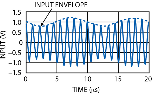
x(t) = cos2πf 1t + a(t)cos[2πf2t + Φ(t)]
where x(t) is illustrated in Figure 2 . The signal phase Φ(t) is set to a constant π/2 purely for illustration. Not surprisingly, the envelope of x(t) fluctuates. In fact the combination of signal and interferer form a periodic wave whose period is 10 µs. The envelope of that wave is shown as the dashed line connecting the carrier peaks in the diagram. Intuitively, the envelope may be conceived as the output of a peak detector on x(t).
The expressions for the envelope E(t) and the resulting limiter output r(t) are derived in Appendix A . Summarizing those results,
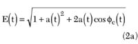
where
(2b)
Φc(t) = relative phase between signal and interferer
Φc(t) = 2π(f2-f1)t + Φ(t)
The limiter output r(t) is by definition x(t)E(t) and is approximated quite closely for a strong interferer by
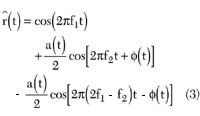
The new frequency component created by the limiter at 2f1-f2 = 800 kHz is shown in Figure 1(b) as part of the limiter output spectrum.
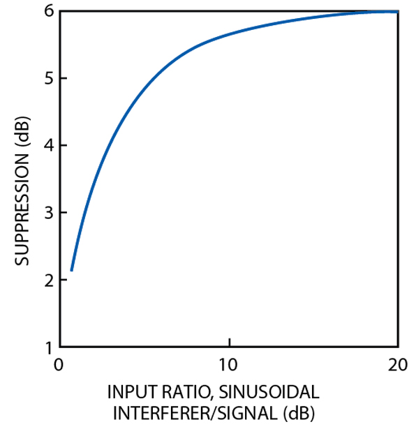
Note that the amplitudes of the original signal component and the newly created 800 kHz component are both 0.1 V, which is half the original signal amplitude. Meanwhile, the output interferer remains at 1.0 V, which means the ratio of the 900 kHz output interferer to the 1 MHz output signal component is 20 dB, as compared with the 14 dB at the input. The 6 dB difference is the classical hard limiter suppression effect. Now, if the input interferer is only moderately stronger than the input signal, the limiter suppression will be less than 6 dB. The strength of the signal and interference components of the limiter output were computed by direct numeric integration at various input power ratios, without use of the approximations leading to Equation 3, and the results were plotted in Figure 3 . This illustrates the degree of limiter suppression experienced over a range of input interferer-to-signal power ratios extending from 0.5 to 20.0 dB. The degree of suppression increases quite rapidly at smaller values of the input power ratio. A more refined interpretation of the limiter's effects can open the potential for abatement of the suppression effect.
Sophisticated Demodulator for Improved Performance
Note that the output component created by the limiter at 800 kHz contains both a(t) and Φ(t) as modulating terms. This suggests the possibility of a more communications-efficient extraction of the signal information by two simultaneous, independent demodulation operations, one at 1 MHz and one at 800 kHz, followed by coherent combination of the pair of demodulator outputs to reconstitute the full-strength demodulated signal as if there had been no limiter. For illustration, assume that the signal is 10 kbps coherent biphase modulated digital data. One bit lasts exactly ten times the period of the input waveform shown previously.
A close inspection of the signal-bearing output components at 800 kHz and 1 MHz is helpful. The modulation format requires that Φ(t) switch between 0 and π depending on the value of the transmitted data bit. Observe also that the practical effect of switching the carrier phase from 0 to -π is exactly the same as switching from 0 to π. Either switch effectively multiplies the cosine carrier by -1 when called for by the data stream. Therefore, in this specific instance, there is no practical difference between seeing +Φ(t) in the second term, right side of Equation 3, and seeing -Φ(t) in the third term. Meanwhile, a(t) is held constant at 0.2 to maintain the initial assumption of a strong interferer-to-signal ratio. Designate bk as the value of the kth data bit, where bk = ±1. The limiter output becomes

where
Tb = 100 µs bit duration
p(τ ) = rectangular bit pulse
where Tb is the 100µs bit duration and p(τ) is the rectangular bit pulse. Implementation of the concept of two simultaneous demodulators necessitates an independent 800 kHz replica of the carrier-acquisition and locking functions found in operation at 1 MHz. As usual, it is assumed that any spurious fluctuations in either f1 or f2 are slow compared with the data modulation rate of 10 kHz. In any case it is clear that the 6 dB suppression effect can be overcome completely by implementing simultaneous demodulators at 1 MHz and 800 kHz, and adding the demodulator outputs coherently.

Note further that in the previous example the implementation of independent demodulators at 800 kHz and 1 MHz requires that the separate data spectra centered at those carrier frequencies be non-overlapping. This requirement was met by holding the data rate to 10 kbps, which causes each replica data spectrum to be narrowly contained near its carrier. But suppose the data modulation is not slow compared to the difference between the input signal carrier and the interferer. Is performance improvement still possible? The answer may still be yes, as illustrated next.
In a second data modulation example suppose the original 10 kbps data signal is converted to a direct-sequence spread-spectrum (DSSS) signal at 500 kchip/s. Thus, each data bit is converted into a 50 chip symbol. Now the data spectrum spans multiplies of 500 kHz, and because the difference frequency between the interferer and the signal carrier is only 100 kHz the spectra of the pair of terms under the summation sign in Equation 4 will overlap considerably, making the use of two independent demodulators impractical. Now it becomes useful to re-express the bracketed term in the summand of Equation 4 in product form such that
(5)
cos(2πf2t) - cos[2π(2f1-f2)t] =
2sin(2πf1t)sin[2π(f2-f1)t]
This suggests an alternate receiver concept that includes a two-step concatenated demodulation. The first step is to acquire f1 and use it to demodulate  (t) by a sin(2π f1t) carrier to yield a "quasi-baseband" signal-bearing term
where
Tss = 2 µs chip duration
ck = chip value ±1
Pss(τ) = chip pulse
Note especially that the product of the sin(2πf1t) demodulating carrier with the leading cos(2πf1t) interferer term in the right hand side of Equation 4 produces identically zero output from the zonal low pass filter that routinely completes the demodulation process. Therefore, only the signal-bearing so(t) appears at the demodulator output. The interferer has been removed by demodulation. The remaining task at hand is to process that signal-bearing term appropriately.
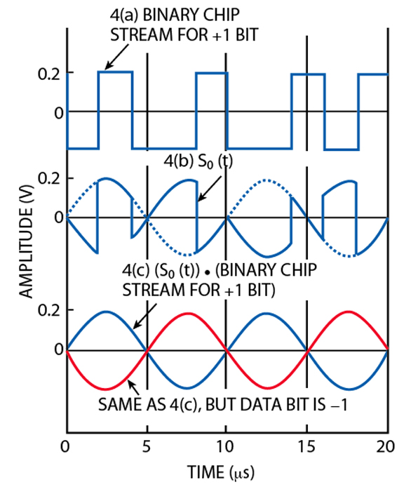
Again, with the reminder that f2 - f1 = 100 kHz, it is clear that the chip modulation rate of 500 kchip/s is much faster than the oscillators observed in sin[2π(f2-f1)t] alone. Therefore, each DSSS chip spans only a fraction of a cycle of the "carrier" at 100 kHz. In practical terms, it is preferable to extract the DSSS signal directly from the right side of Equation 6 as if the latter were a somewhat unusual baseband signal. Several related quantities are illustrated in Figure 4 .
The baseband chip stream, assuming a +1 transmitted bit, appears in Figure 4(a). Its amplitude is 0.2 V, as it would have been demodulated from the signal at the limiter input. Figure 4(b) shows so(t) with 0.2sin[2π(f2-f1)t] superimposed for comparison. Figure 4(c) is the result of multiplying 4(b) by the receiver's unit-magnitude stored chip stream. Here it is assumed that the current information bit is a binary +1, so that the solid graph in 4(c) is a positively signed sine wave. If the transmitted data bit had been a -1, then 4(b) would have been inverted, and the dashed plot in 4(c) would have resulted from multiplication by the stored chip stream.
The receiver, having phase locked to both f1 and f2, now computes sin[2π(f2-f1)t] and decides whether a +1 or a -1 bit was transmitted by deciding whether 4(c) is a positive or a negative sine wave. The communications efficiency with which this decision is made is classically measured by the energy in the 4(c) wave, which is obviously invariant with the sign of the transmitted bit. The degree of limiter suppression is computed in the present DSSS example by comparing the average power in 4(c) with the average power that would have resulted if the receiver had acted on the limiter input instead. If the receiver had accessed the limiter input then 4(c) would have become a constant voltage of magnitude 0.2 rather than the sine wave of peak 0.2 that actually appears in 4(c). That sine wave has just half the average power of the constant 0.2 V; therefore, in this case, the limiter suppression is 3 dB. Once again, a sophisticated receiver, tailored to the circumstances, can improve on the performance otherwise predicted by the classical 6 dB suppression result.
A heuristic grasp of the efficiency of the DSSS receiver can be gained by examination of the phasor diagram shown in Figure 5 . Once again Φc(t) represents the relative phase between the data carrier and the interferer. The signal is resolved into its in-phase and quadrature components, with the in-phase component (in keeping with the definition of Φc(t)) aligned, co-linear with the interferer. When the interferer is much more powerful than the signal, the in-phase signal component a(t)cos[Φc(t)] is simply absorbed into the interferer phasor and therefore vanishes. The quadrature signal component, meanwhile, survives virtually intact. On average, over the constantly changing relative phase between the signal and the interferer, the signal power divides equally between its in-phase and quadrature components. Hence, by inspection, half the signal power is lost in the hard limiting process, which means the DSSS receiver suffers a limiter suppression loss of 3 dB.
Conclusion
The above discussion has suggested, through specific signaling examples, that the classical 6 dB bandpass hard limiter suppression effect can often be abated by customized demodulation methods. Other, possibly superior, receiver strategies than those described here might be conceived and evaluated in the same environments discussed in this article, or in other practical environments. The objective here was not to present a class of universal optimum receivers but to illustrate that the classical 6 dB suppression effect relates generally to a "default" receiver that is not tailored to any specific situation.
If possible, each practical situation should be carefully evaluated on its own footing. In some instances the limiter suppression could even prove to be greater than 6 dB, especially in the case of non-spread data transmission when the data rate is much larger than the difference between interferer and signal carrier frequencies. Generally speaking, a powerful sinusoid is not the only interferer present at the limiter input. Other types of interference, such as thermal noise, may also enter into the performance evaluation. A thorough analysis of the specific signaling situation at hand, considering all manner of performance degradation, is always advised.
References
1. W.B. Davenport, Jr., "Signal-to-noise Ratios in Bandpass Limiters," Journal of Applied Physics , Vol. 24, No. 6, June 1953, pp. 720-727.
2. W.B. Davenport and W.L. Root, An Introduction to the Theory of Random Signals and Noise , McGraw-Hill, New York, NY 1958.
3. C.R. Cahn, "A Note on Signal-to-noise Ratio in Bandpass Limiters," IRE Transactions on Information Theory , Vol. IT-7, No. 1, January 1961, pp. 39-43.
4. N.M. Blachman, Noise and its Effect on Communication , Malabar, Kreiger, 1982. 5. L.B.W. Jolley, Summation of Series, Dover, New York, NY 1961, p. 32, #T117.
|
APPENDIX A As a first step, the limiter input envelope is expressed in complex baseband notation, using the expressions in Figure 5. The input envelope E(t) is a non-negative real quantity, being the length of the hypotenuse of a right triangle whose base is 1 + a(t)cosΦc(t) and whose height is a(t)sinΦc(t). The expression for E(t) is, straightforwardly,
which, upon expansion and collection of terms, becomes
Division of the limiter input by that envelope to produce the limiter output involves expressing 1/E(t) as a series5 expansion, taking the familiar form
Substitution into Equation A3 yields
and the expression for the limiter output becomes the input multiplied by the right side of Equation A4. At this juncture it is convenient to revert to real signal notation, and because a(t) is small compared to unity, the limiter output becomes (A5)
The expansion of the right side of Equation A5 produces more terms in a(t)2 and higher powers. When those, too, are dropped the limiter output becomes (A6)
which reduces, after elementary manipulations, to the desired result,
|
 (A1)
(A1) (A2)
(A2)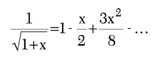 (A3)
(A3)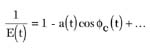 (A4)
(A4)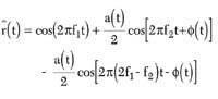 (A7)
(A7)