
The fabricated dielectric-filled waveguide with a silver seed layer was tested using an HP8720D vector network analyzer with the measured results shown in Figure 5. The calibration was done using the HP85052D 3.5 mm calibration kit, where the reference planes are the coaxial cables connected to the device under test. MG Chemicals 842 Super Shield Silver conductive aerosol coating17 with a conductivity of 1.3 x 10⁶ S/m is used as the seed layer for this device. Measured results for the dielectric-filled and air-filled waveguides are shown in Figure 5a and b. The return loss measured for the dielectric-filled waveguide is better than 20 dB across the frequency band of 8 to 10.4 GHz, whereas the air-filled waveguide design demonstrates a return loss better than 20 dB between 9.45 to 10.6 GHz.
A comparison of the air-filled waveguide and coax-to-waveguide loss was given in previous work.12 The insertion loss of the commercial and 3D printed coax-to-waveguide transitions are comparable.12 Once the optimal location for probe feed and depth were achieved, 3D printed two pole air-filled and dielectric-filled filters were designed, additively manufactured and tested to demonstrate the ability to incorporate this approach to practical applications as reported in previous work.12
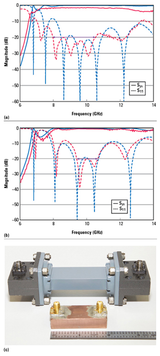
Figure 5 Simulated (blue) and measured insertion loss (red) and return loss of (a) the dielectric-filled waveguide, (b) the air-filled waveguide and (c) assembled size of the conventional 76.2 mm (3 in.) X-Band waveguide with SMA-to-waveguide transitions to the 3D printed copper electroplated air-filled waveguide.12
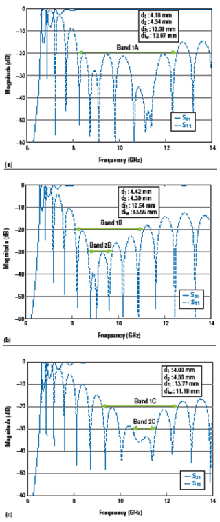
Figure 6 Simulated return loss of the three optimizing designs (a) Design A, (b) Design B and (c) Design C.
Method 2: Addition of Input Coupling Irises
To further improve the return loss across the X-Band frequency, coupling irises are introduced at the input and output of the waveguide past the coax-waveguide transitions, as shown in Figure 3. These irises are similar to those used in iris coupled waveguide filters, though the iris width is much wider than those found in filters, with values just less than the width of the waveguide, a. In previous work,12 it is shown through the additive manufacturing of 3D printed two pole waveguide filters that Method 1 is sufficient for matching coaxial connectors to waveguides for narrow band applications. Method 2 is presented for achieving wider band matching in a compact form.
In Method 2, parameters varied include the probe position, d1, probe depth, d2, iris width, diw, and the iris position from the end of the waveguide, di1. Three designs; A, B and C, are designed to optimize specific bands with return loss better than 20 dB and/or 30 dB. Figure 6 illustrates the simulated return loss obtained for different combinations of parameters. The length of all designs is 100 mm.
The length of the structures for Method 2 is set to 100 mm to limit any input/output coupling and loading between the two coax-to-waveguide transitions. The iris length is set to 12.54 mm, the same iris width used for the 3D printed waveguide filters in previous work,12 thus ensuring the devices are manufacturable. The simulations are performed using the electromagnetic solver ANSYS HFSS.
Design A is optimized for a 20 dB return from 8.2 to 12.4 GHz, with final parameters d1 = 4.18 mm, d2 = 4.34 mm, diw = 13.07 mm and di1 = 12.08 mm. Designs B and C are optimized for a return better than 30 dB across narrower sub-bands, each greater than 1 GHz in bandwidth. Design B has 30 dB return loss from 8.7 to 9.75 GHz (Band 2B in Figure 6b) with final parameters d1 = 4.42 mm, d2 = 4.39 mm, diw = 13.55 mm and di1 = 12.54 mm. The optimized parameters for design C resulting in 30 dB return loss from 10.53 to 11.58 GHz (Band 2C in Figure 6c) are d1 = 4.00 mm, d2 = 4.30 mm, diw = 13.77 mm and di1 = 11.18 mm. Design B and C also have 20 dB return loss bandwidths greater than 2.5 GHz (Band 1B and Band 1C in Figure 6b and Figure 6c).
Results show that this approach, in a compact form, allow the designer to target narrow bands of frequency with return loss better than 30 dB and/or wide bands with return loss better than 20 dB. The addition of the coupling iris in Method 2 allows for wider band match as compared to Method 1 when only tuning the probe position and depth.
Conclusion
Impedance matching methods for 3D printed waveguide designs at X-Band have been presented for dielectric-filled and air-filled waveguides. This design approach eliminates the need for alignment and high-cost SMA-to-waveguide WR-90 transitions necessary for testing and system integration for cascaded RF link applications. The dielectric-filled waveguides include dielectric posts for improved mechanical connection of the SMA connectors. The waveguide devices presented in this article are designed to incorporate the coaxial-to-waveguide transitions permanently within the waveguide design to produce an integrated component with no temporary external transitions required. These designs offer a lower cost, lighter weight design option to their conventional counterparts. Two methods for achieving a good match between the coaxial transmission line and the waveguide are reported. Method 2 includes a coupling iris and offers a compact solution that can achieve 20 dB return loss across the entire X-Band or 30 dB return loss across 1 GHz sub-bands.
Acknowledgments
This work was supported in part by CMC Microsystems for the provision of software tools.
References
- C. Vicente and H.L. Hartnagel, “Passive-intermodulation Analysis Between Rough Rectangular Waveguide Flanges,” IEEE Trans. Microwave Theory and Techniques, 2005, pp. 2515–2525.
- C. Guo, X. Shang, M.J. Lancaster and J. Xu, “A 3-D Printed Lightweight X-band Waveguide Filter Based on Spherical Resonators,” IEEE Microwave Wireless Components Letters, 2015, pp. 442–444.
- G.L. Huang, S.G. Zhou, C.Y.D. Sim, T.H. Chio and T. Yuan, “Lightweight Perforated Waveguide Structure Realized by 3D Printing for RF Applications,” IEEE Transactions on Antennas and Wave Propagation, 2017, pp. 3897-3904.
- S. Khan, N. Vahabisani and M. Daneshmand, “A Fully 3D Printed Waveguide and Its Application as Microfluidcally-controlled Waveguide Switch,” IEEE Transactions on Components, Packaging and Manufacturing Technology, 2017, pp. 70–80.
- F. Cai, W.T. Khan and J. Papapolymerou, “A Low Loss X-Band Filter using 3D Polyjet Technology,” IEEE MTT-S International Microwave Symposium, 2015, pp. 1–8.
- C. Guo, J. Li, J. Xu and H. Li, “An X-band Lightweight 3D Printed Slotted Circular Waveguide Dual-mode Bandpass Filter,” IEEE International Symposium on Antennas and Propagation USNC/URSI National Radio Science Meeting, 2017, pp. 2645-2646.
- R. Dahle, P. Laforge and J. Kuhling, “3D Printed Customizable Inserts for Waveguide Filter Design at X-band,” IEEE Microwave Wireless Component Letters, 2017, pp. 1080-1082.
- M. Bozzi, C. Tomassouni, L. Perregrini, R. Bahr and M. Tentzeris, “Additive Manufacturing of Substrate Integrated Waveguide Components,” IEEE International Symposium on Antennas and Propagation USNC/URSI National Ratio Science Meeting, 2015, pp. 1522-3965.
- G. McKerricher, A. Nafe and A. Shamim, “Lightweight 3D Printed Microwave Waveguides and Waveguide Slot Antenna,” IEEE International Symposium on Antennas and Propagation, USNC/URSI National Radio Science Meeting, 2015, pp. 1322–1323.
- M. D’Auria, W.J. Otter, J. Hazell, B.T.W. Gillatt, C. Long-Colins, N. M. Ridler and S. Lucyscyn, “3D Printed Metal-pipe Rectangular Waveguides,” IEEE Trans. Components, Packaging and Manufacturing Technology, 2015, pp. 1339–1349.
- R. Mirzavand, H. Saghlatoon, M.H. Honari, M. Ye and P. Mousavi, “A Light-weight Low-cost 3D Printed Waveguide for Medium Power Applications,” International Applied Computational Electromagnetics Society Symposium, 2017.
- J. Kuhling, R. Dahle, D. Chowdhry and P. Laforge, “Applying Additive Manufacturing to Integrate Coaxial Connectors with 3D Printed Waveguides for Cascaded RF Link Applications,” Additive Manufacturing, Vol. 35, 2020.
- W. Yi, E. Li, G. Guo and R. Nie, “An X-band Coaxial-to-Rectangular Waveguide Transition,” IEEE International Conference on Microwave Technology & Computational Electromagnetics, 2011, pp. 129–131.
- J. Li et al., “A Full X-Band Fully 3-D Printed E-Plane Rectangular-Coax-to-Waveguide Transition,” IEEE MTT-S International Microwave Symposium, 2019, pp. 1209–1212.
- M. Durga, S. Tomar, S. Singh and L. Suthar, “Millimeter wave In-line Coaxial-to-Rectangular Waveguide Transition,” IEEE Applied Electromagnetics Conference, 2011, pp. 1–3.
- Stratasys - FDM Technology, 2019, Web, http://wwww.stratasys.com/3d-printers/technologies/fdm-technology.
- MG chemicals, 2017, Web, http://www.mgchemicals.com.
- “132147 Datasheet,” RF Amphenol, Web, https://www.amphenolrf.com/132147.html.
- High Frequency Simulation Software, ANSYS, 2018, Web, www.ansys.com/products/electronics/ansys-hfss.