
There is certainly no shortage of information about designing power amplifiers these days, and several books address the subject quite admirably.1-6 However, as well as these books cover the theory and underlying logic of such designs, they do not tell the reader precisely how to do it. As a result, most designers develop their own ad-hoc methodologies for such designs, which can vary significantly in effectiveness.
This article describes a thorough design methodology that leverages advances in electronic design automation (EDA) and test and measurement data to improve the probability of first pass success. It is not the only way to design a power amplifier, but experience has proven it to be quite effective. It is based on the use of simple analyses and measurements to obtain all the necessary information before the design commences; the design then becomes a relatively simple process of creating a few simple building blocks, and connecting them together. The most important part of the design is a methodical evaluation of the power device. As an example, a single-stage, half-watt, HBT power amplifier is designed. Additionally, the latest load pull analysis capabilities in Microwave Office™ 2002 software are incorporated, as well as using this tool for simulation, layout and design verification. Version 5.02, the latest release, provides a number of new features that support a more thorough PA design methodology quite well. They will be described in the following sections.
The Amplifier
The goal is to design a single-stage heterojunction bipolar transistor (HBT) amplifier integrated circuit. The amplifier must cover 1.6 to 2.1 GHz, have at least 22 dB gain at full output and operate at a power-supply voltage of 3.4 V. To save chip area and minimize output loss, the output matching circuit is off-chip. An HBT process from Global Communication Semiconductors Inc. (GCS) will be used. The GCS foundry offers indium gallium phosphide (InGaP) HBT technology, having an fmax of approximately 50 GHz. The DC bias regulator will also be off-chip, using a CMOS IC. Thus, the output matching network and DC bias need not be part of the MMIC design.
The design of the amplifier starts at the output and proceeds toward the input. The process is as follows: evaluate the device using nonlinear analysis and load pull simulations; determine the device size, bias point and optimum load; determine the device input impedance; synthesize an input matching network; connect the input network to the device and make sure the combination works properly; and design the output matching network. Each step is addressed in that order.
Evaluate the Device

Before beginning the design, it is essential to perform a "sanity check" on the device models that the foundry typically provides. Many foundries use the SPICE Gummel-Poon (G-P) model to characterize their devices due to the fact that the model is uniformly supported across all circuit simulators. G-P is an older model and has many limitations for HBT design. More advanced models, such as the UCSD HBT model7 and Anholt HBT model, are implemented in Microwave Office 2002 design software, along with the MEXTRAM and VBIC models.
Nevertheless, such advanced models are not uniformly supported, so many foundries only extract G-P models. Thus, users will probably be using G-P for HBT modeling well into the foreseeable future.
It is particularly dangerous to design RF and microwave circuits without understanding the models used in the design. There is certainly adequate information available on SPICE models, especially G-P.8 Often, parameters just "don't look right," and questionable parameters should be resolved before the design begins. It is a simple matter to evaluate the device.
Two simple test circuits are used, as shown in Figure 1. The same RF test circuit can be used to calculate both S-parameters and power performance; no special set-up is necessary other than to create graphs for the desired quantities. The device's small-signal current gain and maximum available gain are also calculated to make sure they are close to the expected ft and fmax advertised for the device. Figure 2
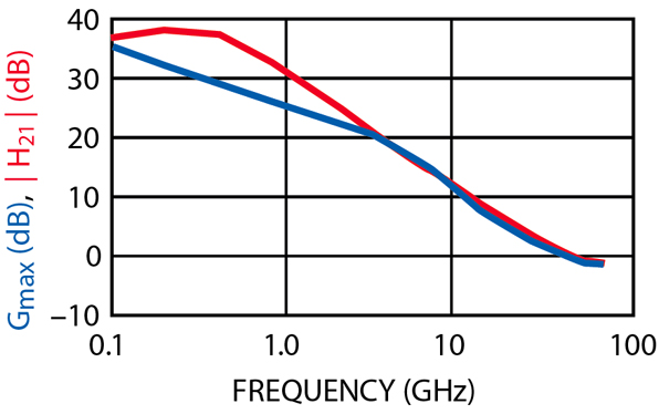
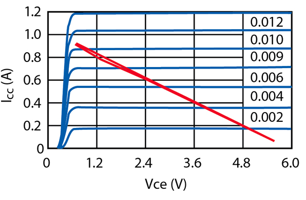
shows the current gain, H21, and the maximum available gain Gmax, indicating ft and fmax of 45 GHz, in good agreement with the expected 50 GHz. To make certain that any potential instability problems do not exist, stability circles are computed. Finally, the HBT's I/V characteristics are swept to make certain that the DC part of the model is reasonable, and to determine the base bias current that provides the proper collector bias current. The I/V characteristics are shown in Figure 3.
Determine the Device Size, Bias Point and Optimum Load
Beginning with the load impedance, for a class-A amplifier, the resistive part is given by the well known relation,
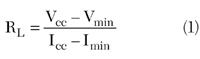
and the output power, Pout, is
Pout = 0.5 (Vcc-Vmin)(Icc-Imin) (2)
where
Vcc = bias voltage
Icc = bias current
Vmin = minimum collector-to-emitter voltage
Imin = minimum collector-to-emitter current
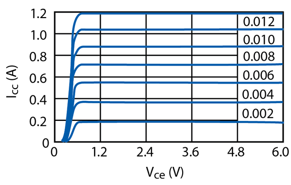
The device's I/V curves show that Vmin is approximately 0.5 V, and the estimated Imin is approximately 0.05 A. Noting that Vcc = 3.4 V, and experimenting a little, Icc = 0.5 A. This results in Pout = 0.65 W and RL = 6.4 Ω. These are starting values, and may have to be modified somewhat.
According to the foundry, the current density in the devices must be limited, under bias conditions, to 25 kA/cm2. The individual cells have areas of 50 µm2, so a device having 40 cells is needed. The foundry offers a 20 cell device, so two of these can be used in parallel.
In most power amplifier designs, a shunt inductance must be provided to resonate the device's output capacitance. However, from S-parameters, it is found that, at this relatively low frequency, the output capacitance is negligible, so no reactive tuning is needed. The load is purely resistive.
Now the harmonic-balance simulator is used to optimize the bias and load impedance using the RF evaluation circuit shown previously. No attempt has been made to match the input at this time; the excitation is simply increased until maximum output power is achieved. The load impedance is adjusted while monitoring the collector waveforms and adjusting the power.
It is a simple matter to do this with the "tune" mode; numerical optimization, although available, is not necessary. The optimum condition is achieved when both the voltage and current minima are near zero, but not clipping. If the resulting output power is not right, the bias current and load resistance are adjusted until the correct power is achieved. Note that an extra fraction of one dB in output power is allowed to compensate for losses in the output matching network.
The final collector current is 0.47 A and load resistance is 5.0 Ω.
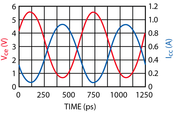
Figure 4 shows the collector voltage and current waveforms. These are internal quantities; that is, they are the current in, and voltage across, the collector-to-emitter controlled source. It is essential to calculate the voltage and current at this point, not at the terminals.
The terminal quantities include voltage drop across the collector and emitter resistances, and current in any output capacitance that might exist. Thus, it is impossible, by viewing external quantities, to know whether the load is optimized.
In this case, the internal voltage and current exhibit a precise 180° phase difference, showing that the output reactance is negligible (or if it were not negligible, proper output tuning) and no saturation or clipping. Figure 5 shows the dynamic load line. Its lack of ellipticity also indicates that there is no significant reactance in the output.
As a final test, a load pull simulation of the device is performed using the "load pull wizard" in the simulator. (A wizard in Microwave Office 2002 software is a separate software program that controls the simulator through an interface based on Microsoft's component object model (COM)).
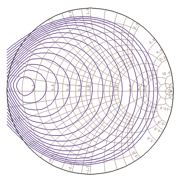
COM is a software technology that allows versatile interaction between separate software modules. Figure 6 shows load pull contours of output power. These indicate that the load impedance is indeed optimized, and that the circuit is not unduly sensitive to the load.
Determine the Input Impedance
The Microwave Office 2002 design suite enables the operator to calculate a large-signal input impedance, Zin(ω). This is defined as
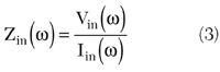
where Vin(ω) and Iin(ω) are the input voltage and current Fourier components at the excitation frequency. This is the device input impedance that should be used for designing a matching circuit.
To design a matching circuit, it is helpful to have a lumped-element model of the HBT's input impedance. The dominant input elements in the HBT model are the base resistance and collector-to-emitter capacitance, so it is no surprise that a series RC network models the input impedance quite well.
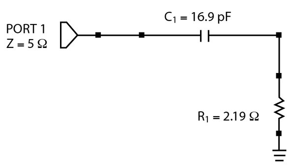
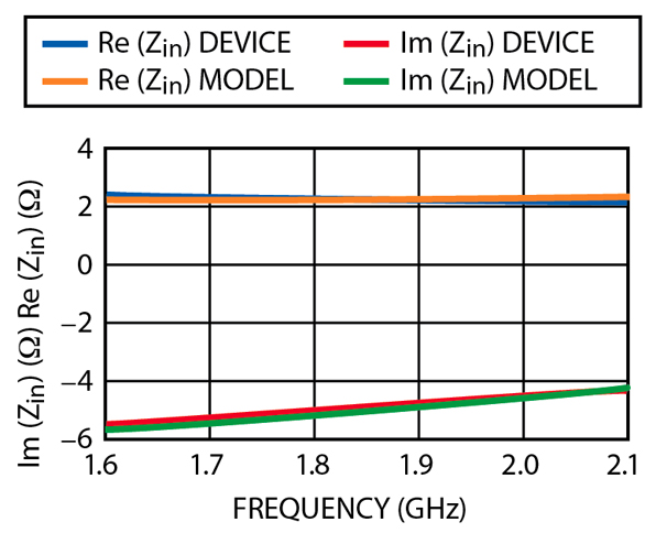
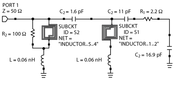
By plotting the input impedance of the HBT and the model on the same graph, the model can be easily adjusted to fit the input impedance. Again, optimization could be used for this task, but it is a simple, two-minute job with the tuner. The input model, consisting of 16.9 pF and 2.2 Ω, is shown in Figure 7, and a comparison of the measured and modeled impedances is shown in Figure 8.
Synthesize the Input Matching Network
Several considerations drive the design of the input network. To eliminate low frequency gain, it should have a high pass structure, and should allow for easy biasing and DC blocking. Because of the high Q of the load, and the need to transform from a very low impedance to 50 Ω, the design of the network is not simple.
To meet these requirements, a series-L, shunt-C design is used. A "constant-Q" approach is employed, in which elements are selected by moving along a contour of constant Q on the Smith chart.
This is an entirely graphical process which can be performed with Microwave Office 2002 software using the "real-time tuning" mode. Additionally, resistive loading is used to optimize the input match over the relatively wide bandwidth of 1.6 to 2.1 GHz.
The loading introduces loss, of course, but the gain of modern HBTs is so great that it is acceptable. It also reduces the sensitivity of input return loss to uncertainties in the device model.
Once the element values are found, the inductances are replaced, one at a time, with square-spiral inductors, re-optimizing the circuit after each inductor is replaced. For best accuracy, the inductors should be analyzed by a planar electromagnetic (EM) simulator.
Conventional lumped-element models of foundry devices are often less accurate and do not allow the designer to customize and optimize his own inductors or capacitors. For this task, the integral EMSight™ electromagnetic simulator in the Microwave Office design suite is used.
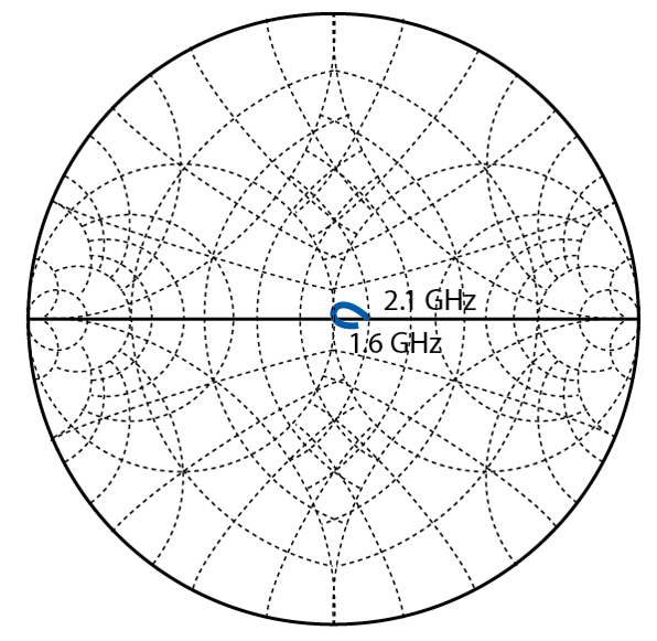
The EMSight simulator will generate and export a SPICE equivalent circuit of the rectangular spiral inductor, so it is easy to determine whether the inductor has the desired value. Figure 9 shows the current and electric field analysis for a four and a half turn spiral inductor. Figure 10 shows the final matching circuit which resulted in an input return loss of better than 20 dB across the 1.6 to 2.1 GHz band.
Connect the Matching Circuit to the HBT
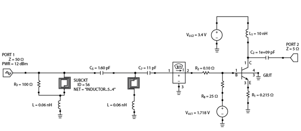
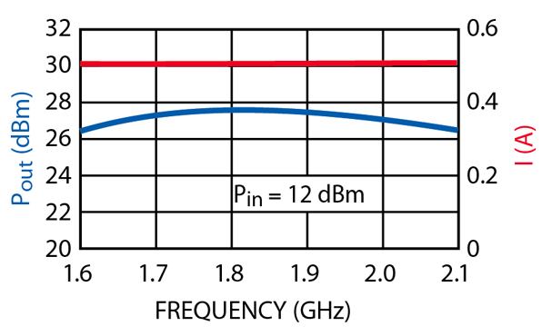
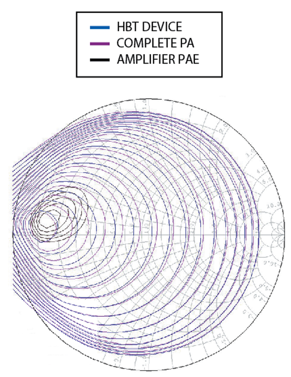
Now the matching circuit is connected to the HBT, and the combination, shown in Figure 11, is analyzed. Figure 12 shows the input reflection coefficient, and Figure 13 shows the output power and bias current without any further tuning or optimization of the circuit. In Figure 14 , a set of load pull contours for the complete amplifier is shown, which is very similar to the one for the device alone.
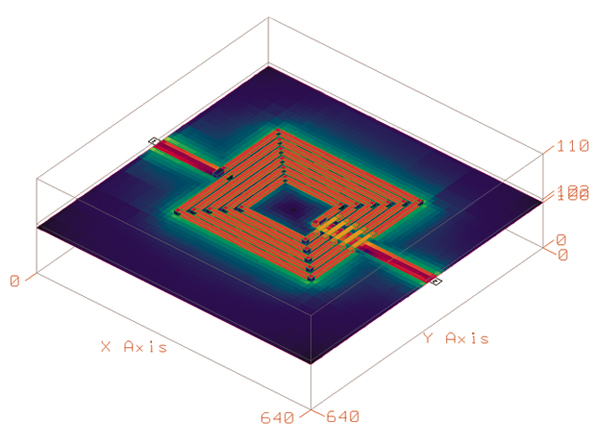
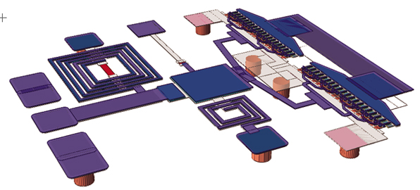
Finally, Figure 15 shows the amplifier layout, which was also produced using the layout capabilities in the Microwave Office software. The 40 cell HBTs were realized as two 20 cell devices in parallel, and the inductors and capacitors are readily identifiable.
Design the Output Matching Circuit
The output matching circuit is not part of the chip design, but an amplifier will not work very well without one. Because of the low load impedance required by the amplifier, an output matching circuit is unavoidably lossy.
Most of the loss is generated where the currents are greatest, in the elements closest to the chip. Ideally, these should use capacitive microstrip stubs, but size limitations may dictate the use of chip capacitors instead. In this case, the main problem is a trade-off between capacitor cost and Q.
A second problem is the large impedance transformation between 5 Ω at the chip and the invariably 50 Ω outside world, which creates a direct trade-off between bandwidth and loss.
It was found that a matching circuit consisting of series transmission lines and shunt capacitors represents a good trade-off between loss and size.
High quality RF ceramic chip capacitors are used. The chip must also be designed to allow the use of multiple bond wires, as even bond-wire loss can be significant.
Conclusion
In designing power amplifiers, the combination of a methodical approach and the use of modern CAD tools allows a designer to produce a valid design with minimal effort.
The MMIC design methodology becomes extremely efficient when the designer has access to a single CAD environment that provides EM simulation, harmonic balance, load pull analysis and integrated foundry libraries for laying out the chip.
The key to the process is to determine as much as possible about the power device to be used in the amplifier before the design itself begins. The old saying, "knowledge is power," applies here more than you might imagine.
AWR, the AWR logo and Microwave Office are trademarks of Applied Wave Research Inc. All other marks are the property of their respective holders.
References
1. S.C. Cripps, RF Power Amplifiers for Wireless Communication, Artech House Inc., Norwood, MA 1999.
2. J.L.B. Walker, High Power GaAs FET Amplifiers, Artech House Inc., Norwood, MA 1993.
3. N. Dye and H. Granberg, Radio Frequency Transistors: Principles and Practices , Butterworth-Heinemann, Newton, MA 1993.
4. S. Maas, Nonlinear Microwave Circuits, IEEE Press, New York, NY 1997.
5. L. Larson, RF and Microwave Circuit Design for Wireless Communication, Artech House Inc., Norwood, MA 1996.
6. G. Gonzalez, Microwave Transistor Amplifiers, Prentice-Hall, Englewood Cliffs, NJ 1984.
7. UCSD High Speed Devices Group, "HBT Model Equations," http://hbt.ucsd.edu/.
8. P. Antognetti and G. Massobrio, Semiconductor Device Modeling with SPICE, McGraw-Hill, New York, NY 1988.
Dr. Stephen A. Maas received his BSEE and MSEE degrees in electrical engineering from the University of Pennsylvania in 1971 and 1972, respectively, and his PhD in electrical engineering from UCLA in 1984. Since then, he has been involved in the research, design and development of low noise and nonlinear microwave circuits and systems at the National Radio Astronomy Observatory, Hughes Aircraft Co., TRW and the Aerospace Corp. He is now chief scientist at Applied Wave Research Inc. (AWR), where he specializes in nonlinear circuit simulation technology. For several years he was a member of the electrical engineering faculty at UCLA, where he still periodically teaches regular and extension courses.
Ted Miracco received his bachelor of science degree in electrical and computer engineering from Carnegie-Mellon University in 1987. He is a co-founder and the executive vice president of Applied Wave Research Inc. (AWR), an El Segundo, California-based company that was founded in 1994. He has worked in microwave product development for over a decade, specializing early on in microwave filter design. Before joining AWR, he was a senior account executive at Cadence and, prior to that, was responsible for business development and worldwide corporate accounts at EEsof. He can be reached via e-mail at miracco@mwoffice.com.