
Beamforming is a phased array technique that enables mobile communications base stations to focus higher power in the direction of user equipment (UE), providing higher signal-to-noise ratio (SNR) and increased data rate. It can also prevent signal degradation from interfering transmitters by nullifying their signals, so mobiles can share the same spectrum with other networks and increase spectral efficiency. This article describes an eight-element linear monopole array designed for and tested at 1.8 and 2.6 GHz. Results meet the goals for steering capability, null and sidelobe suppression and multibeam formation.
The world’s demand for connectivity is rapidly increasing, with mobile subscriptions expected to approach nine billion by the end of 2025, of which some 2.6 billion will be 5G.1 Supporting this fast growing market requires upgrades to operator infrastructure. Beamforming, a well-known technique in defense radar and military communications systems, is being adopted for commercial mobile communications. Beamforming can be thought of as spatial multiplexing. Antenna array elements are weighted in phase and amplitude to modify the radiation pattern as desired. These modifications may be interactive, as in the case of adaptive arrays, or based on predefined switched beams. With beamforming, a base station can direct its antenna gain to communicate efficiently with other devices in the system, while isolating itself from interferers. Spectrum sharing is also possible. Two communication standards operating at the same frequency will not interfere with each other, since each can place beam pattern nulls in the direction of the other.
Global System for Mobile Communications (GSM) was the first attempt to apply beamforming to mobile communications. A base station equipped with an adaptive antenna array processor, allowing full beam uplink and downlink adaptation in every GSM frame, was proposed and tested by Kuchar et al.2 For LTE, beamforming was introduced in 3GPP release 10.3 The standard supports passive arrays with horizontal beamforming and active arrays with 2D and 3D beamforming. Beamforming is becoming more important in the subsequent releases of 3GPP. The 5G new radio (NR) defined in release 15 relies on beamforming and beam management,4 and the 5G NR description considers the possibility of exploiting beamforming in the uplink and downlink transport channels.5 Beamforming requirements are discussed, such as null suppression and steering angle range.6 Digital beamforming enables the efficient evaluation of direction of arrival (DoA) beamforming algorithm performance.
A complete system for testing steering capability, null and sidelobe suppression and multibeam formation using various digital beamforming algorithms is presented in this article. The system is based on commercial transceivers from Analog Devices.7
SYSTEM DESCRIPTION
This system implements beamforming in the digital domain. Calculated complex weights are applied to the received signals at baseband, which requires a complete receiver chain. The system is designed to operate at the LTE-A and 5G NR bands from 1.7 to 1.9 GHz and from 2.5 to 2.7 GHz.8 5G NR includes sub-6 GHz bands, referred to as FR1 and mmWave bands, designated FR2.9
The number of array elements determines the directivity of the main beam and its half-power beamwidth. As the number of elements increases, the directivity increases and half-power beamwidth decreases.10 This test bed comprises an eight-element antenna array, an RF front-end and a field-programmable gate array (FPGA) digital processor (see Figure 1). The antenna array is composed of wideband monopoles linearly distributed with uniform inter-element spacing. RF signals transmitted by the UE are received by the antenna array. These signals have different phases and amplitudes, depending on the position of the UE relative to the base station. Dynamically weighting the received signals produces maxima and nulls in the radiation pattern, determined by the weights. This system can evaluate and test the performance of horizontal beamforming algorithms, as well as the performance of new algorithms. To do this, eight full receiver chains are used, with the eight I/Q pair outputs digitized for post processing. The beamforming weights are calculated and applied to the digital baseband signals in the FPGA. Summation of the weighted signals provides the best SNR at the angle of the main beam and the worst SNR at the angle of the null in the radiation pattern.
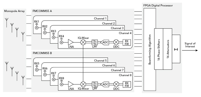
Figure 1 Beamforming test bed.
MONOPOLE ANTENNA ARRAY
CST Microwave Studio 2017 was used for the design and simulation of the antenna array.11 The single element is a monopole with a rectangular shape and rounded vertices of radius Rcor1. The monopole is printed on Rogers RO4003C 0.06 in. thick, which has a relative dielectric constant of 3.38 and loss tangent of 0.0027 (see Figure 2). It is fed from an edge-mounted SMA connector through a 50 Ω microstrip line. The transition between the feed line and the rectangular antenna element is elliptical, with a minor axis length Lgap. The width of the element and its length are Wmono and Lsub, respectively. The antenna is backed by a leaf-like ground plane of width Wgnd and length Lgnd. The dimensions used in the design are Wmono = 57 mm, Lmono = 36.5 mm, Rcor1 = 9 mm, Lgap = 6.5 mm, Wgnd = 57 mm and Lgnd = 24 mm. The ground surface is modified with 10 corrugations in the bottom edge to minimize coupling to the coax. The antenna has a metallic reflector 44 mm from the substrate to direct the antenna’s power in the boresight direction. Confirming the monopole’s performance, Figure 3a shows the simulated and measured impedance matching from 1.7 to 2.7 GHz, and Figure 3b shows the simulated and measured H-plane radiation patterns at 2.6 GHz.
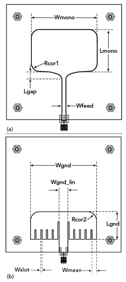
Figure 2 Top (a) and bottom (b) of the single element antenna.
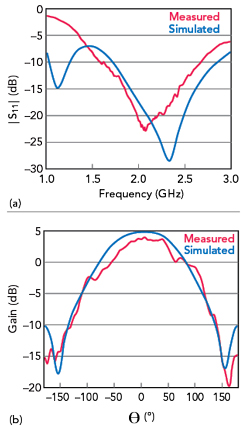
Figure 3 Simulated vs. measured performance of the single element antenna: |S11| vs. frequency (a) and 2.6 GHz E-plane pattern (b).
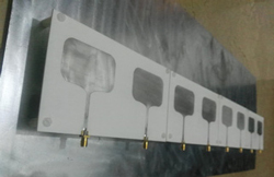
Figure 4 Eight-element monopole array.
For horizontal beamforming, the single monopole is extended to a linearly distributed eight-element array with uniform element spacing (see Figure 4). Because the antenna is wideband, the choice of inter-element spacing was challenging. The separation was set to 83 mm, which is a half-wavelength at 1.8 GHz. The eight elements are uniformly fed using a Mini-Circuits ZB8PD-362-S+ eight-way power divider. Figure 5 shows the simulated and measured radiation patterns at 1.8 and 2.6 GHz with each element uniformly excited.
RF FRONT-END
Because beamforming is performed digitally, a complete receiver chain is needed. The Analog Devices AD9361 wideband receiver was selected, as it meets most common communication standards, including LTE-A, contains two separate receive chains and operates from 70 MHz to 6 GHz.12 As the demonstration system requires eight receiver channels to capture the signals from the eight antenna elements, the full receiver uses two Analog Devices’ FMCOMMS5 transceiver boards with dual FMC connectors, compatible with the Zynq ZC702 FPGA board from Xilinx (see Figure 1). Each transceiver board has four dedicated receiver channels driven by a single local oscillator (LO), requiring two transceiver boards for the eight receive channels.
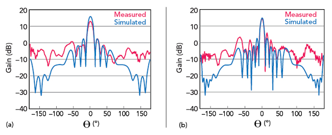
Figure 5 Monopole array H-plane patterns at 1.8 (a) and 2.6 (b) GHz, simulated vs. measured.
To evaluate digital beamforming in the uplink, weights are applied to the received signals. The signal coming from the antenna element passes through a coaxial cable into an internal low noise amplifier. The amplified signal is down-converted by a mixer, and the I/Q signal pair is digitized by a 12-bit, third-order, continuous time delta-sigma modulator analog-to-digital converter (ADC). After digital down-conversion and filtering with a decimation finite impulse response filter, the signal is ready for post processing.
In digital beamforming, the relative phase between elements is critical. If the eight receivers are not synchronized in phase, accurate post processing beamforming is not possible. There are two challenges: the first, to ensure that all LOs are at the same frequency; the second, to ensure all are synchronized in phase. The LO driving both transceivers in each AD9361 chip is an Analog Devices ADF5355BCPZ phase-locked loop (PLL) with integrated VCO. A 40 MHz temperature compensated crystal oscillator (TCXO) is used as the PLL reference clock.
If the four PLLs were driven from the same reference clock and configured with the same N-divider, all the PLLs would oscillate at the same frequency. Each of the two transceivers on the same FMCOMMS5 board are driven by the same PLL. To synchronize the two transceiver boards, the TCXO reference clock on one, the master, is buffered with an ADCLK846B fanout buffer and passed via a coaxial cable to the external reference input of the other board, the slave (see Figure 6). This locks the two PLLs at the same frequency. However, while the RF paths for the eight channels are almost identical, there is still a length difference between the paths, in addition to the path difference between the master and slave boards.
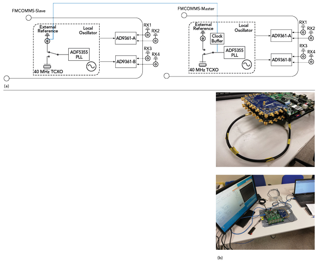
Figure 6 Master/slave setup (a) for synchronizing the phase between the two FMCOMMS5 boards (b).