
Noise is a limiting factor for sensitive reception. In recent communication receivers, noise, along with many external factors, including intermodulation, reciprocal mixing and spurious response, may disturb the sensitive reception of the desired signal. Thus, much consideration for the noise and other factors that disturb the signal reception and their analysis are required in the receiver design procedure to keep the SNR of the received signal above a desired level for the reconstruction of the signal.1-3
In this article, an equation which can simplify the system level design of a receiver is introduced, and some important SNR degrading factors in the receiver are reviewed. An example of a system level design of a receiver meeting the CDMA2000 standard is then offered.4
The basics of noise factor
The noise factor, F, of a system is defined as
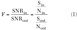
In Equation 1, the input noise power Nin is the available noise power at the conjugate matched input impedance, at an ambient temperature of 290 K. Typically the input impedance of the receiver for wireless communication is 50 Ω with negligible reactance. With the assumption of negligible reactance, the input noise power Nin may be written as
Nin = kTB = -174 + 10logB dBm (2)
where
k = Boltzman constant
T = absolute temperature
B = bandwidth of the desired signal5
To distinguish this fundamental input thermal noise from others it will be called Nin0 .
Added noise in a noisy system
To understand the relation between a system's noise factor and the added noise by the system at the output, consider the system in Figure 1 , with a gain G and a noise factor F. When the signal Sin and the noise Nin0 are applied at the input, the output signal Sout and the output noise Nout are
Sout = GSin (3)
Nout = GNin0 + Na (4)
where
Na = added noise by the system
and the noise factor F is

and with this noise factor F, the added noise Na is represented as
Na = GNin0 (F-1) (6)
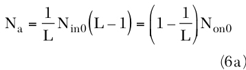
For lossy systems like filters, the system's gain is 1/L and the noise factor is L. Thus the added noise Na for a lossy system may be represented as
Using the above relation between Na and F, the F of a cascaded system can be easily derived. Let the gain and noise factor of each stage be G1 , F1 and G2 , F2 (Figure 2 ). At the output of the first stage, the signal and noise powers are:
S1 = G1Sin (7)
N1 = G1 Nin0 + Na1 = G1 Nin0 + G1 Nin0 (F1 -1) = G1 F1 Nin0 (8)
and at the output of the second stage
Sout = G2 S1 = G1 G2 Sin (9)
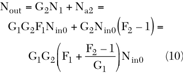
Thus the noise factor of the cascaded system is
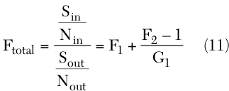
Extending Equation 11 to a multi-stage system, the well-known Friis' equation is obtained.
Receiver Noise Equation
Normalized Input Referred Added Noise
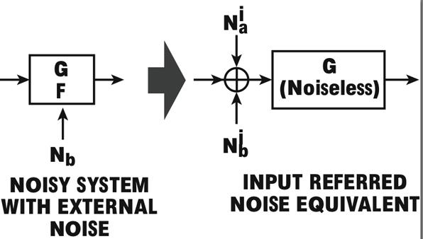
To make sure of a system's ability to receive a weak signal, its noise characteristics are usually expressed in terms of an equivalent input noise power.6 Figure 3 shows that a noisy system may be expressed by a noiseless system and an equivalent input referred noise source.
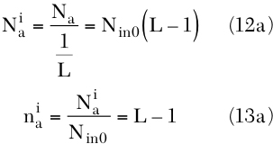
From Equation 6, the input referred added noise  is given by

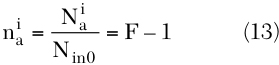
By dividing both sides of Equation 12 by Nin0 and defining a new parameter, the normalized input referred added noise  , the following equation is obtained:
This simple equation can be adapted for passive systems with some modifications. In passive systems, the loss L and the noise factor F have the same value, thus the input referred added noise and the normalized input referred added noise are respectively
Receiver Noise Equation
To develop a receiver design method using added noise analysis, several SNR degrading factors (excluding NF), such as intermodulation products, reciprocal mixing products, spurious responses and transmitter leakage noise, must be considered. These factors cannot be distinguished from the desired signal when they happen to be in the desired signal band, and they are independent from one another. Thus, in a wide sense, they can be treated as noises in receiver design.
When considering more than two SNR degrading factors, the input referred noise equivalent model with multiple noise sources must be used. Figure 4 shows the input referred equivalent of a system with two different noise sources. The SNRout of this system is
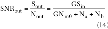
Since SNRin is Sin /Nin0 ,
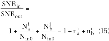
Equation 15 represents the SNR degradation in the system by two noise sources. When there are M noise sources, Equation 15 will become:
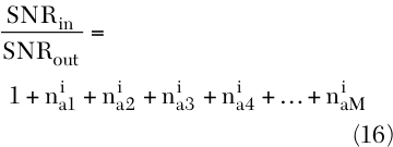
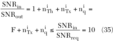
Equation 16 is called the receiver noise equation. Naturally, one of the noise sources is the thermal noise, which is characterized by a noise factor. If each noise source can be identified and the allowable SNR degradation is known, the receiver's specifications using this receiver noise equation can be easily determined.
Noises in an RF Receiver for Wireless Communications

As stated before, all independent SNR degrading factors are treated as noises. They can then be categorized as intrinsic or extrinsic, according to whether their cause is inside or outside the receiver (see Table 1 ).
Intrinsic Noise = Thermal Noise
Thermal noise is the most fundamental noise in RF receivers. It originates from the noise performance of each component and is characterized by NF. The input referred thermal noise is
Ni Th = Nin0 (F-1) (17)
Transmitter Noise Leakage in Receiver Band
When the transmitter operates near its maximum output power, it generates a significant broadband noise, and some fraction of that noise is added to the receiver's input noise through the imperfect isolation of the duplexer. Using Equations 4 and 6,
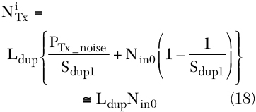
where
PRx_noise = noise power of the transmitter in the Rx band
Sdup1 = duplexer's isolation from Tx to Rx
Ldup = insertion loss of the duplexer from antenna port to Rx port
The approximation made in Equation 18 holds for sufficiently large Sdup1 .
Cross-modulation Product
Cross-modulation occurs mostly in CDMA receivers when the desired signal is accompanied by a single strong interferer. The amount of noise that the cross-modulation product adds can be calculated as
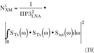
where
STx(ω ) = transmitted signal's frequency spectrum
Sint(ω ) = interferer's frequency spectrum
B = frequency range where the cross-modulation product overlaps the desired signal
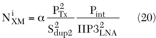
However, from a review of the cross-modulation problem in CDMA cellular and CDMA PCS,7,8 a simpler representation of Equation 19 can be written as
where
PTx = transmitter power
Pint = interferer power
Sdup2 = duplexer's isolation at TX band
α, which is called a soaking factor,8 represents the proportion of overlap area between the cross-modulation product and the desired signal for all cross-modulation products. Typically, the value of α is between 0 and 0.5.
Reciprocal Mixing Product
When the receiver processes the desired signal with the existence of a strong interferer in an adjacent channel, reciprocal mixing may become a problem. The magnitude of the reciprocal mixing product in the desired signal's band can be obtained by integration over the overlapped frequency range. However, if the frequency of the interferer offset from the center of the desired signal is sufficiently large, the reciprocal mixing product's effect is usually estimated assuming a flat band phase noise2,9 as
Ni RM ≈ Pint · PN · B (21)
Intermodulation Product
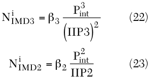
When the desired signal and two interferers, which are allocated in the frequency domain such that their intermodulation product may arise in the desired signal band, pass through the receiver system, the intermodulation product of the interferers may disturb the reception of the desired signal. The effect of the intermodulation product may appear in a few different forms such as third-order intermodulation, adjacent channel power (ACP) of an adjacent channel modulated interferer and second-order intermodulation. Their amounts can be expressed in mathematical form as Equations. As the ACP of a modulated signal is also a kind of third-order intermodulation, it can be represented by the same expression as the third-order intermodulation product.
where
β 3 = β 2 = 1 for intermodulation product
β 3 and β 2 < 1 for ACP
according to the overlap bandwidth with the desired signal.10 Note that the second-order intermodulation product is a problem for a homodyne architecture rather than a heterodyne architecture. The second-order distortions of the modulated signals may be an important issue for the homodyne type receiver design and will be considered in DC offset noise.
Image (Heterodyne Architecture)
The image problem is a unique problem in a heterodyne receiver and its magnitude can be represented as
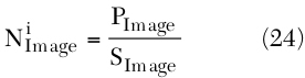
In Equation 24, the SImage refers to the image rejection performance of the receiver. This performance is mostly achieved by using a duplexer and an image rejection filter. In some modern receivers, the image rejection performance of the receivers may be achieved by the use of image rejection mixers.
DC Offset (Direct Conversion Architecture)
When a homodyne architecture is considered, the DC offset and 1/f noise are important noises. DC offset comes mainly from LO self-mixing and second-order nonlinearity of the system, and occurs at and around DC. If the DC offset at exactly DC is rejected by the DC offset cancellation technique, the remaining noise is mostly the second-order distortion around DC and can be represented as
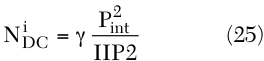
where γ has a value between 0 and 1. Especially for the CDMA signal, when it is modeled as a sum of multi-tones,11 γ is 3/64.
The 1/f noise, which may be another problem in a homodyne receiver, must be considered specifically when the receiver is designed with a CMOS process,5,6 and is not considered here.
Quantization Noise
The ADC's noise performance is often characterized by SNR, which describes the maximum value of the ratio of the output signal power to quantization noise power. It may be obtained when the input signal level is exactly the full-scale range (FSR) of the ADC. The SNR of an N-bit ADC is represented as
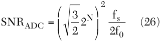
where
f0 = upper frequency limit of the desired signal
fs = ADC's sampling rate
2f0 = Nyquist sampling rate
The input referred quantization noise power,  , in the desired signal band can be represented using the SNR values in Equation 26 as
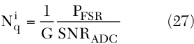
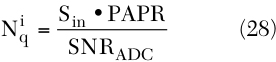
Since the input signal level of an ADC is usually adjusted to the FSR of the ADC, the total gain in the receiver, G in Equation 27, can be regarded as
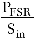
in the case where the input signal is a sinusoid. However the digitally modulation signals' power may be time-variant, and in this case G is
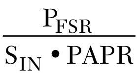
where
PAPR = peak to average power ratio of the desired signal
Substituting this value for G in Equation 27 yields
With the assumption of a rapid variation of the input signal, the quantization noise can be regarded as an independent random variable uniformly distributed between ±1/2 LSB. It can then be treated as a white noise whose power is within the frequency band of ±1/2fs .12
Imperfectly Filtered Interferers
Strong interferers (besides intermodulation products and their reciprocal mixing products) themselves may disturb the reception of the desired signal. They act like noises and degrade the SNR at the input of the digital demodulator. The contribution of the imperfectly filtered interferers to the input referred noise of the receiver can be represented as
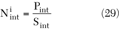
In the above equation Sint is the channel selectivity of the receiver.
System Level Design of the Receiver for CDMA2000
With the knowledge of the effect of noises in the receiver, it can now be designed using the receiver noise equation. An example of a receiver design is shown in the following.
CDMA2000 is a candidate standard for third-generation personal communications, IMT2000. The standard document from 3GPP24 states several test conditions, which define the receiver's minimum required performance in the worst communications environments.
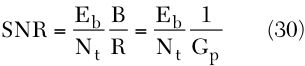
In the documents, the receiver is verified by the FER performance, and the FER performance is directly related to the Eb /Nt at the receiver back-end. The achievable minimum SNR value can be obtained from the CDMA equation.13

The tests are recommended for signals with a 9.6 or 14.4 kbps data rate, and the receiver's specifications are derived here for signals with a 9.6 kbps data rate. In the following, the considerations made in the design of a receiver are shown for a few important test conditions (see Figure 5 ). Note that for the convenience of calculation, decibel scales are used in the derivations.
Receiver Sensitivity
From the sensitivity test conditions, the signal and noise powers at the input of the receiver can be found as
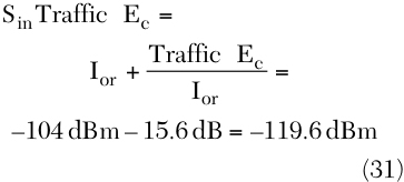
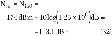
Thus the input SNR is
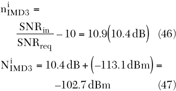
SNRin = -119.6 dBm - (-113.1 dBm) = -6.5 dB (33)
To keep the FER less than 0.001, the Eb /Nt must be over 4.5 dB, so from Equation 30, the required minimum SNR is
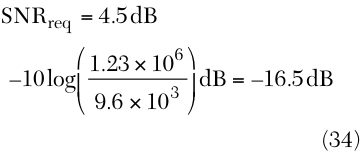
Thus the SNR degradation by the system must be less than SNRin / SNRreq , which has the value of 10 dB (=10) in this example. In the sensitivity test condition, there is no interfering signal but the transmitter signal. Looking into this test situation, four noise sources are found: the input thermal noise, receiver added thermal noise, transmitter noise leakage in Rx band and quantization noise. Thus the receiver noise equation, concerning the noise sources listed above, is
When the receiver is designed, the ADC is chosen carefully not to degrade the receiver's performance. In typical CDMA receivers, the ADCs are often with 4-bit resolution and a sampling speed of eight times the data rate (8f0 ), then from Equations 26 and 28, the quantization noise's contribution is given by:
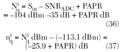
Since the CDMA signals typically have a PAPR of 12 dB,14  has a value of -13.9 dB. Compared with the allowable SNR degradation of 10 dB, it is small enough to be ignored. Thus, Equation 35 can be rewritten as:
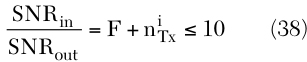
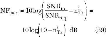
From Equation 38 the noise factor requirement of the receiver can be found as
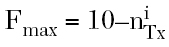
or
Since the typical noise power of a CDMA transmitter in the Rx band is -135 dBm/Hz,1 if the duplexer's Tx-Rx isolation is larger than about 50 dB, then  ≈ 1 and Fmax ≈ 9 or NFmax ≈ 9.5 dB.
Single-tone Desensitization
In this test condition, the input signal power is increased by 3 dB from the sensitivity test condition, which corresponds to a SNRin of -3.5 dB. The FER requirement is loosened to be 0.01, which corresponds to Eb /Nt of 4.3 dB or SNRreq of -16.7 dB.
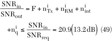
There are some other noise sources besides the noise sources considered in the sensitivity test: the reciprocal mixing product, cross-modulation product and the imperfectly filtered interferer. Thus, the noise equation can be stated as
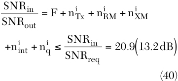
Then with the assumption that the receiver just meets the requirements of the sensitivity test and the interferer is sufficiently suppressed by channel filtering, the contribution of the reciprocal mixing product and cross-modulation product to the receiver's input referred noise can be calculated as
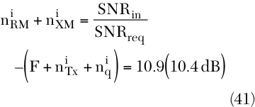
Ni RM + Ni XM = 10.4 dB + (-113.1 dBm) = -102.7 dBm (42)
If it is assumed that there is only a small cross-modulation product which can be ignored and the phase noise PN(ω ) is flat in the band of interest, the phase noise can be written as
PN = -102.7 dBm - (-30 dBm) - 10log(1.23 x 10⁶ Hz) ≅ -133.6 dBc/Hz @ 1.25 MHz offset (43)
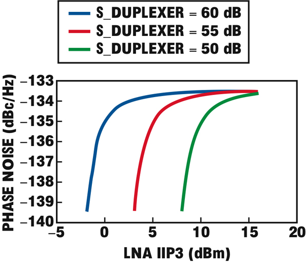
However, in a real case, the linearity of the LNA and the isolation of the duplexer are not ideal and the cross-modulation must be considered. Therefore, some trade-offs between the phase noise of the receiver and the LNA's linearity are needed. Figure 6 summarizes the trade-offs for the case of a 24 dBm transmitter power (mobile class 3) and the duplexers with three different isolations. α is set to be -5.6 dB, the same value as the PCS case.7
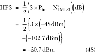
Intermodulation Spurious Response
In this test, the receiver noise equation can be written as
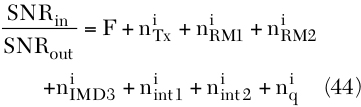
However, the reciprocal mixing products can be ignored in this test because of the small interferer power (18 dB less than that in the single-tone test) and larger frequency offsets. Knowing that the SNRin is the same as that in the single-tone desensitization test, and taking the assumptions made in the analysis of single tone desensitization test, Equation 44 may be simplified as
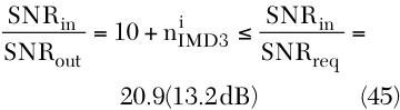
Then the contribution of the intermodulation product to the receiver's input referred noise is
Therefore, the IIP3 of the receiver must be larger than the value stated in the equation:
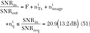
Adjacent Channel Selectivity
In this case, the situation is very similar to the single-tone desensitization test, but the cross-modulation product can be ignored since it comes from the receiver's third-order nonlinearity and will occur within the 3.75 MHz bandwidth around the center of the modulated interferer tone and doesn't overlap with the signal. Thus, the receiver noise equation can be written as
Then by using Equation 22 with the approximation of one tone at 1.875 MHz offset and flat band phase noise, the phase noise requirement can be derived as
PN = -102.7 dBm - (-37 dBm) - 10log(1.23 x 10⁶ Hz)dB = -126.6 dBc/Hz @ 1.875 MHz offset (50)
Observing this result the phase noise requirement for this case is found to be looser than that of the single-tone desensitization test. However, the time-variant power level of the interferer with the receiver's nonlinearity may cause instantaneous problems.
Receiver's Blocking Characteristics
From the blocking test of the receiver the image rejection requirement of the receiver can be determined. Typically, the IF of the receiver is from several tens to a few hundred megahertz. In that case the maximum interferer power, which can exist, is -15 dBm. The receiver noise equation in this case is
From the above equation, the minimum required image rejection performance is determined to be 87.7 dB.
Conclusion
There are many SNR degrading factors in a receiver for wireless communication: receiver thermal noise, intermodulation product, reciprocal mixing product, Tx leakage noise and so on. The SNR degrading factors are independent of each other and can be treated as noises from the viewpoint of SNR. Then the receiver can be modeled as a two-port system with multiple noise sources.
In this article, a two-port noisy system was reviewed using added noise concept, and the receiver noise equation was developed by extending this concept. Some important SNR degrading factors in a receiver were summarized and an example of a system level design of a receiver was shown using the receiver noise equation.
References
1. W.Y. Ali-Ahmad, "RF System Issues Related to CDMA Receiver Specifications," RF Design , September 1999, pp. 22-32.
2. O.K. Jensen, et al., "RF Receiver Requirements for 3G W-CDMA Mobile Equipment," Microwave Journal , Vol. 43, No. 2, February 2000, pp. 22-46.
3. H.S. Shin, et al., "System-level Performance Analysis and Design of RF Receiver for W-CDMA User Equipment," ICMMT 2000, Beijing, China, September 2000, pp. 319-322.
4. 3GPP2, C.S0011-A "Recommended Minimum Performance Standards for CDMA2000 Spread Spectrum Mobile Stations," Third Generation Partnership Project2 (3GPP2), March 30, 2001.
5. B. Razavi, RF Microelectronics , Prentice Hall, 1998.
6. P.R. Gray and R.G. Meyer, Analysis and Design of Analog Integrated Circuits , Third Edition, John Wiley & Sons Inc., New York, NY 1993.
7. R. Mohindra, "Cross-modulation and Linearization in CDMA Mobile Phone Transceivers," Seventh Annual Wireless Symposium, San Jose, CA, February 22-26, 1999.
8. B.K. Ko, et al., "A Nightmare for CDMA RF Receiver: The Cross-modulation," AP-ASIC 99, 1999, pp. 400-402.
9. J.C. Rudell, et al., "Recent Developments in High Integration Multi-standard CMOS Transceivers for Personal Communication Systems," UCB Electronics Research Laboratory Memorandum: UCB/ERL M97/82, 1997.
10. Q. Wu, et al., "Linear RF Power Amplifier Design for CDMA Signals: A Spectral Analysis Approach," Microwave Journal , Vol. 41, No. 12, December 1998, pp. 22-40.
11. J.C. Pedro and N.B. de Carvalho, "On the Use of Multi-tone Technique for Assessing RF Components' Intermodulation Distortion," IEEE Transactions on Microwave Theory and Techniques , Vol. 47, No. 12, December 1999, pp. 2393-2402.
12. D.A. Johns and K. Martin, Analog Integrated Circuit Design , John Wiley & Sons Inc., New York, NY 1997.
13. A.J. Viterbi, CDMA: Principles of Spread Spectrum Communication , Addison Wesley Longman Inc., 1995.
14. J.S. Lee and L.E. Miller, "Analysis of Peak-to-average Power Ratio for IS-95 and Third Generation CDMA Forward Link Waveforms," IEEE Transactions on Vehicular Technology , Vol. 50, No. 4, July 2001, pp. 1004-1013.
 Hyung Joun Yoo received his BS degree in physics from Seoul National University, Seoul, South Korea, in 1979, and his MS and PhD degrees, also in physics, from the Korea Advanced Institute of Science and Technology in 1990 and 1994, respectively. He worked for the Agency for Defense Development from 1979 to 1982, and in 1983 joined ETRI, where he served as director of the advanced technology research department. Since 1998 he has been a professor at the Information and Communications University (ICU). His research interests include RF systems for mobile communications, RFICs and nonlinear analysis of RF circuits.
 Ji-Hoon Kim received his BS degree in electrical engineering from Seoul National University, Seoul, South Korea, in 1998, and his MS degree, also in electrical engineering, from the Information and Communications University (ICU) in 2000. He is now enrolled in the PhD program at ICU. His research interests include RF systems for mobile communications and RFICs.