
As the complexity of wireless systems grows and requirements become more demanding, the task facing analog/RF engineers is not getting any easier. In today's rapid-paced working environment, time-to-market demands accurate and fast results from device simulations. To meet these demands for the effective management and analysis of design data requires robust simulations that deliver informative results, with accuracy and precision.
What has been prevalent in many organizations is to define design flows rigorously with a limited and unique set of software, including schematic and layout editors as well as other utilities. This is beneficial in terms of design flow management, but can result in a limited set of analysis and simulation tools. The drawback, of course, is that to connect an external simulator to an established design framework can require a lot of tailoring and consulting work from the parties involved.
The APLAC Simulation Builder (ASB) 1.1 introduces an entirely different concept to address these concerns. Instead of implementing a single simulator in a standard design flow the versatile simulator integrates to many standard, industry-strength frameworks with a robust and simple mechanism.
Role of ASB
Simulators are almost always driven by a combination of netlist definitions (components and sources joined by named nets) and analysis definitions. In this case, though, the simulator possesses the strength and singular programmability to achieve demanding and automated simulation and optimization tasks. It bridges the gap between a variety of EDA CAD frameworks and the simulator.
This approach enables designers to map their third-party schematic data into the simulator input using an organized set of mapping rules, managed by an easy-to-use graphical interface. Framework-specific adapters enable the flexible and robust transfer of design data from the CAD framework to the simulator's input file, providing access to a complete, accurate and integrated set of analog simulation methods. What's more, once set up, the mapping process is completely transparent to the user.
Designs imported using the simulation builder work automatically with every analysis method performed by the simulator, including DC, AC, time domain and harmonic balance analyses, and with full noise, sensitivity, optimization and statistical analysis support. Designs can also be simulated using integrated plug-in modules like RFIC or system simulation options.
Features of ASB 1.1 include the use of as many mapping libraries as needed, the creation of master and user specific rules, the ability to keep hierarchical and primitive rules separate, and all relevant windows feature online help capability.
A Recent Files List aids hierarchical planning, affording fast access to ASD files, and ASD templates enable new simulation definitions around the netlist to be entered from a catalog. It is also possible to duplicate an existing template and move templates relative to each other, and errors and mapping libraries can be exported to HTML for reference.
To illustrate how the ASB 1.1 functions, consider how it fits into the design cycle. Recognizing the fact that designers may use third-party CAD frameworks for schematic design and versioning as a matter of course, Mentor Graphics Design Architect (MGDA), Cadence Virtuoso and Innoveda PowerLogic based frameworks are covered.
Therefore, when a design is ready for functional verification, the ASB simulation manager is used to extract component and connectivity data to a transition netlist, through a fully automated framework-specific adapter. Mapping rules can be stored in category-specific mapping libraries, using a graphical user interface to tailor the simulator input.
The Simulation Manager then automatically processes extracted netlist data, mapping each element onto the simulator input according to pre-defined mapping rules, which can be re-used each time an element is implemented in another design. Should the mapping contain any missing element types or other errors, a diagnostic report is generated.
The designer can use the Simulation Manager to combine netlist input with analysis and output parameters, completing the simulator input file and launching the simulation. This is processed and the desired output data shown using graphical windows or text windows, or saved as graphical or text files. The data can also be back annotated automatically in the Innoveda framework. After simulation, the original CAD framework can be used to re-version the design and generate layouts. The altered schematic can be run through the same simulation with the press of a button.
That is the theory but the best way to illustrate the practice is by example. The three frameworks covered - Cadence Virtuoso, Mentor Graphics DA and Innoveda PowerLogic - will be used as examples.
Cadence Virtuoso Example
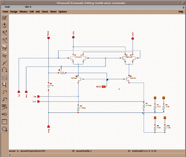
Mixers are commonly implemented in ICs in modern radio devices such as mobile phones, so consider a mixer circuit consisting of Gilbert cells in differential configuration (see Figure 1 ). In this example, the RF signal is at 900 MHz, and the LO frequency is at 800 MHz.

APLAC comes with several nonlinear analysis methods, including transient, harmonic balance, large-signal/small-signal and others. Here, what is used is a classical two-tone harmonic balance (HB) scheme with a nonlinear device defined in the Cadence framework. Nonlinear characteristics such as gain variations relative to input power, input impedance variations and nonlinear noise are easily analyzed. The degree of tonality (one-tone, two-tone...) and number of intermodulation products is limited only by the available computing power.
All blocks in this IC mixer example are built using only standard Cadence analogLib elements, implemented and parameterized hierarchically. For ASB 1.1, the schematic and its elements remain completely intact inside the framework and require no alteration, and the elements' netlisting properties are defined completely inside the simulation builder.
For example, the Mapping Rule shown in Figure 2 is used to transfer analogLib's "RES" element to an APLAC resistor.
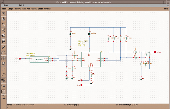
The block is placed into a hierarchical element (mixer), used in upper-level hierarchy with matching and biasing circuitry signal nets (RF input, local oscillator plus and minus nets, and output) are denoted by named pins (nets). With ASB 1.1, each hierarchical element is netlisted separately, using the simulator's DefModel concept (see Figure 3 ).
Among other results, the relationship of the inductance values to the input impedance of the mixer as different power levels are fed to the mixer can be studied. Figure 4 shows five different inductance values with input power levels from -15 dBm to +5 dBm.

MGDA Example
Consider the design of a practical RF element to be designed using the simulator, with Design Architect as the front end. The structure, a branch line hybrid (shown in Figure 5 ), is symmetric respective to both X and Y axes.
The lengths and widths of the microstrip branch lines are easy to calculate with hand calculations, but their exact measurements can easily be checked as specified through optimization.
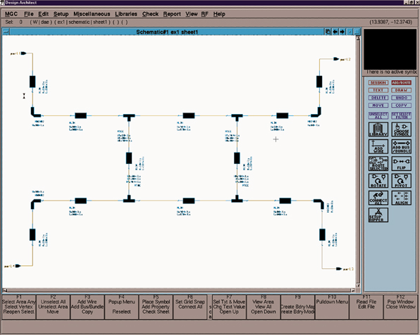
In this study, the structure is specified to operate at 1.8 GHz on an FR4 substrate with ε r = 4.0 and h = 0.7 mm (Z0 = 50 Ω ), yielding a quarter wavelength of 23.74 mm. The RF elements are added from the RF Architect's ADS library, and then connected and parameterized by their RF-specific attributes.
The performance of the branch line hybrid is simulated by adding simple APLAC language statements, such as port definitions and sweep statements, to the list of simulation controls. The Simulation Manager is also used to launch the simulation, and the desired results are delivered as text and/or graphics, and can be saved as text or graphical output files.
Innoveda PowerLogic Example

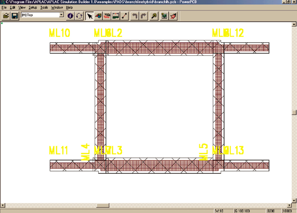
The RF design capabilities of certain design frameworks are not geared for RF design tasks but they can be extended. An example is the APLAC RFKit for Innoveda PowerLogic/PCB framework, by which it is possible to parameterize schematic transmission line elements (such as microstrip lines) and then reflect the length and width attributes to the layout side so that the shape matches the attributes of the schematic element. This is shown in Figure 6 , and the resulting branch line hybrid layout is shown in Figure 7 .
Conclusion
ASB 1.1 integrates industry-strength simulation technology with external design frameworks, providing an independent, objective test-bench for verification of any device under development. This approach requires no internal libraries in the CAD framework. Design data is used to generate simulator input, using mapping libraries customized with a simple graphical user interface, while simulations can be created and managed easily using ASB simulation wizards.
In all, users of industry-strength design frameworks can have a completely new approach to their existing analog/RF schematics and tailor their design flows towards a more productive analysis and design functionality.
APLAC Solutions Oy,
Helsinki, Finland
+385 9 5404 5000,
www.aplac.com.
Circle No. 300