
mmWave systems will have a key role supporting the massive data rates planned for 5G networks. However, unfavorable propagation and technical limitations challenge the feasibility and adoption of such systems. Addressing these challenges, Gapwaves is developing waveguide technology with superior performance over conventional printed circuit board (PCB) solutions, including exceptional efficiency, routing, subarray partitioning, filtering, isolation and thermal handling. With improvements in performance, range, number of components and power consumption, the hardware, deployment and operating costs can be significantly reduced. This article discusses the design principles and results of Gapwaves’ demonstration platform, including both passive and active measurements, and the integration of high-power GaN semiconductors to further enable the vision of high performance and cost-effective mmWave systems.
5G, the next-generation mobile network, has a large set of ambitious objectives, leveraging multiple technologies for several different application scenarios.1 Within those, the 100x increase in network capacity compared to the current 4G network will be the most visible to the consumer. Traditional sub-6 GHz frequencies will continue to be the backbone for ubiquitous connectivity, with a boost in capacity from additional bands and advances in coding. However, such a dramatic increase in data rates heavily depends on massive amount of spectrum: GHz of bandwidth available in the mmWave region at a lower cost per Hz. Regulatory bodies have identified several bands for this, mostly between 24 and 60 GHz.
Moving to the mmWave region raises technical issues. The coverage from a base station is considerably less than that of existing systems, due to large propagation losses and severe shadowing and penetration effects from obstructions by buildings, trees and people. mmWave active components generate low output power with low efficiency, with smaller size creating problems with component and power density. This results in limited transmit power, high power consumption and expensive components. Typically, all components suffer from increased losses with frequency, which can become onerous for planar technologies at high frequencies. Also, satellite and backhaul services coexist in the mmWave region, requiring RF filters to prevent interference, which increases system losses.
Deployment of 5G mmWave systems will be driven by household fixed wireless access (FWA) first, with mobile access later. The success of the former depends on base station coverage; to strengthen the business case in suburban areas, higher inter-site distance (ISD) and equivalent isotropic radiated power (EIRP) are needed.2 Higher EIRP increases capacity in systems with hybrid and digital beamforming, where the additional power can be shared across multiple beams and users.
mmWAVE APPLICATIONS
The industry response to the above challenges has mainly been planning small cell, high capacity coverage. However, while a denser deployment will be unavoidable, the economic feasibility and widespread availability depends on the technical solutions and associated cost. The number of base stations per area determines the cost for equipment, deployment and operation.
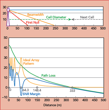
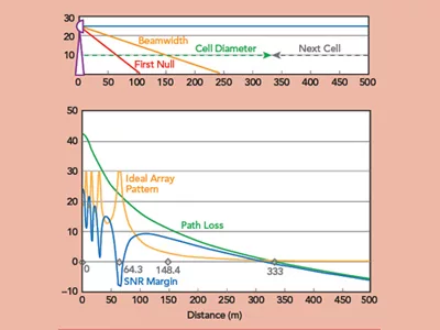
Figure 1 SNR margin relative to the cell edge for an 8-element vertical subarray with no downtilt and 333 m cell radius.
Recently, the first demonstration products were released by major telecommunications equipment manufacturers.3 Most of the current systems are based on integrated PCB antennas, typically with a patch array on the front of the board and active components on the back side. Losses are minimized by vertically routing through the PCB in a one-feed-per-antenna configuration, at the expense of low gain. As a result, achieving high EIRP and downlink coverage are challenging. To partially compensate, a large number of active chains are used, increasing the cost of the system and the power consumption. However, the increased power at the base station, as opposed to the gain, does not help the uplink, which is the hardest leg. The tight integration and high power consumption in a very limited space of a multi-layered PCB create thermal handling and complexity issues. Another challenge is integrating filters and their impact on performance, which is substantial at these frequencies. All these limitations ultimately result in poorer performance, reduced range, higher power consumption and increased cost. The solution by some suppliers is to increase the system size, resulting in a large number of expensive components.
Taking a different approach, Gapwaves is focusing on maximizing antenna gain and minimizing feed and filtering losses, to increase system range and performance and increasing component output power. Most importantly, low loss subarrays can be used to increase gain, with the trade-off of reduced elevation coverage, as the beam narrows and grating lobes appear. In real scenarios, however, a user’s angular distribution in elevation is extremely limited, especially for suburban FWA with low buildings. As shown in Figure 1, even an 8-element, vertical subarray with no downtilt or elevation scanning provides adequate signal level at all distances for a 500 m ISD (333 m cell radius), despite an elevation beamwidth of about 12 degrees. This is valid as long as no deep notches are present in the elevation pattern.
WAVEGUIDE REVISITED
Figure 2 Imperfect joints in standard waveguide cause leakage and spurious modes (a) compared to the fields in a Gapwaves waveguide (b).
The primary transmission technologies for microwave applications are metal waveguide and substrate-based PCBs. While the former offers unmatched performance, its bulkiness, cost and complexity have limited applications to niche, high-end markets such as satellite and military. PCBs offer planar, robust, cost-effective solutions with satisfactory performance and, for these reasons, have long been the standard for commercial solutions.
However, both technologies face severe challenges at mmWave frequencies. PCB losses are substantial: at 30 GHz, conventional PCB microstrip lines with high frequency substrates suffer losses in the 10s of dB/m, compared to fractions of dB/m for waveguide. PCB designers must compensate by using premium substrates and minimizing trace lengths; however, as frequencies increase, the losses become overwhelming. Waveguide suffers from increasingly impractical manufacturing tolerances as frequencies increase. A rectangular waveguide with a joining defect on the order of micrometers between its two parts suffers catastrophic leakage (see Figure 2a). Split-block design best practices and high quality joining processes improve performance but are not suitable for mass manufacturing.
A solution is offered by Gapwaves, a robust and low loss technology developed at Chalmers University of Technology by Professor Per-Simon Kildal and his research group.4 By using an artificial magnetic conductor surface, typically realized with a bed of pins, robust waveguide-like transmission lines and components can be created without needing electrical contact between the layers. As shown in Figure 2b, the equivalent Gapwaves waveguide performs flawlessly with a gap present, containing the fields within a few rows of pin and with comparable losses. No joining process is necessary. This key aspect enables a waveguide to achieve both premium performance and cost-effective manufacturing for consumer markets. Gapwaves AB was founded in 2011 with the objective of developing and commercializing Gapwaves waveguide solutions.
GAPWAVES WAVEGUIDE 5G ANTENNA
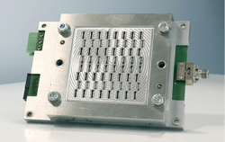
Figure 3 Gapwaves 28 GHz demonstration array.
To demonstrate the advantages of Gapwaves waveguide, we have developed a demonstration platform including the key passive and active components, although the focus is on the antenna and RF performance (see Figure 3). Typical requirements have been considered; as a result, the design is not tailored for any specific application.
The center frequency is 28 GHz, in line with U.S. 5G trials, and the target bandwidth is greater than 13 percent to accommodate current 5G bands. A 1.2 GHz filter is integrated in each subarray feed to support analog, digital and hybrid beamforming and the typical instantaneous bandwidths. Full scanning is provided in azimuth and reduced in elevation. A spacing of λ/2, approximately 5.5 mm, and 4-element vertical subarrays were adopted to guarantee ±45 and ±10 degree scanning in azimuth and elevation, respectively. The demonstration antenna is an 8x8 array. Although a smaller size, it is sufficient to fully characterize the system and extrapolate to larger sizes without unnecessary complexity. Due to the subarrays, 16 feeds are present. SiGe front-ends are used, which provide a total EIRP of 44 dBm based on typical SiGe RFIC performance.
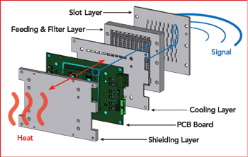
Figure 4 Exploded view of the Gapwaves waveguide array.
As shown in Figure 4, the system is a multi-layer, largely metal assembly. The PCB, with the active components, is located between the shielding layer on the back and the cooling layer on the front. The shielding layer improves isolation and cavity mode suppression, and the cooling layer hosts the transitions to the antenna. Both layers are key to thermal performance. From the PCB, the RF is routed to the filter and distribution layer, which provides low loss routing, the subarray feeds and dedicated filters. Finally, the slot antenna is the front layer.
Transitions
One of the key advantages of Gapwaves waveguide technology is the low loss nature of its interconnections, typically more than 10x better than equivalent PCB solutions. It is highly desirable to transition from the PCB hosting the digital and low frequency signals to waveguide as soon as the RF signal is generated, performing high frequency functions such as filtering and routing in waveguide. The transition between PCB and waveguide should guarantee a low loss, robust and contact-less interface.
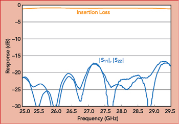
Figure 5 Back-to-back measurement of the transition through a four-layer FR4 board.
While a variety of transitions have been designed and manufactured, a through-substrate configuration has been adopted. This allows positioning the components facing backward in direct contact with the heatsink. Since the signal travels from the microstrip vertically through the substrate, different transition versions have been designed depending on the PCB stack-up. A single transition with a two-layer 10 mil Rogers RO4350 board has a measured insertion loss of 0.2 dB and return loss of 20 dB over a 20 percent bandwidth. Figure 5 shows a back-to-back measurement of a four-layer board with a 10 cm waveguide line section. Tolerance analysis and repeated measurements prove the robustness of the design to assembly variations.
Filtering
RF filters are needed to protect sensitive services, such as the passive Earth Exploration Satellite Service (EESS).5 The EESS band extends to 24 GHz, and the low end of the 5G n258 band starts at 24.25 GHz - only 1 percent frequency margin. Meeting emission limits requires sharp filter rejection or an expensive guardband. While several filter technologies could be applied, they can introduce considerable loss, use scarce PCB area and cause complicated routing.
Gapwaves waveguide technology enables waveguide filters integrated in the antenna, offering premium performance and eliminating complexity. While waveguide filters are well known and used in high performance applications, the amount and density of the filters pose the main challenges for the gap waveguide design. Achieving the filter area, constrained by the antenna element spacing to approximately 0.5λ x 2λ, is extremely challenging, as the area includes the division walls or pins between the subarrays and transitions between layers. Since the array will contain tens to hundreds of filters which must be functional as assembled without tuning, the design must be extremely robust to manufacturing and assembly. While the pin structure of the Gapwaves waveguide helps with the robustness, the design of the filter resonator is crucial. The design for meeting these requirements is less than about λ/2 in x, y and z.
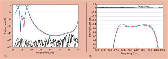
Figure 6 Measured performance of two 28 GHz Gapwaves waveguide bandpass filters showing wideband performance (a) and passband insertion loss (b).
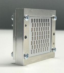
Figure 7 The single polarization Gapwaves antenna is an 8 x 8 slot array configured as 4-slot subarrays in eight columns and two rows.
For the demonstrator antenna array, the filter design is a third-order Chebyshev with 1.2 GHz bandwidth (20 dB return loss) centered at 28 GHz. The measured performance of two filters is shown in Figure 6. The insertion loss is 0.4 dB, compared to an equivalent microstrip filter which would have losses of several dB. Although the filter fits comfortably under each subarray, for these measurements it was positioned on the auxiliary through line to characterize the filter independent of the antenna.