
There is growing interest and development activity for devices and systems that operate at mmWave frequencies. So much, that a billion mmWave devices are projected to be produced annually in 2023.1 The growth is being driven by several emerging applications (see Figure 1). In the U.S., fixed wireless access and 5G networks are being deployed at 28 and 39 GHz. A recent FCC auction included spectrum at 48 GHz, and 3GPP’s release 17 is looking at frequencies to 71 GHz. There’s also a corresponding interest in high speed wireless backhaul networks using E-Band (71 to 86 GHz), W-Band (92 to 114 GHz), even D-Band (130 to 175 GHz). Discussions about 6G propose using 95 GHz and above. Non-cellular standards such as WiGig, or IEEE 802.11ad, operate around 60 GHz and radar sensors in smartphones also operate at 60 GHz.2 The use of automotive radar sensors, primarily at E-Band, is increasing to support autonomous driving. IMEC has demonstrated a 140 GHz radar sensor that can be used for gesture recognition or non-contact driver or patient monitoring.3
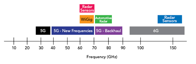
Figure 1 Primary mmWave applications.
Whether for communications or sensors, many mmWave devices use antenna arrays, which come in many varieties depending on the requirements. They may only have a few elements or hundreds, single or dual polarization, simple patches or complex radiating elements. At mmWave frequencies, connecting the transceiver or beamformer IC to the array is important, with loss, impedance control and isolation optimized.
Despite the interest in mmWave, it is challenging to build small and cost-effective systems at these frequencies. While semiconductor design and process technologies have made considerable advances, packaging and module integration technologies can limit mmWave integration. In this article, we review the options for packaging and module integration at these high frequencies, including low temperature cofired ceramic (LTCC), antenna in package (AiP), fan-out wafer level packaging (FOWLP) and PolyStrata®. Comparing them, we discuss how each of these solutions address:
- Signal loss
- Thermal performance
- Small size and high isolation
- Support for heterogeneous integration
- Scalability
Approaches for mmWave Packaging
Packaging technologies are distinguished by the process, dielectric substrates and integration of passive elements, active die and ASICs. Each technology has advantages and hurdles when used for RF system on chip packages at mmWave frequencies. The main drivers for these packaging technologies are commercial markets - 5G and IoT - and ease of manufacturing. The packaging techniques discussed here are being considered by industry for commercial wireless product development and are assessed for use in mmWave systems.
LTCC
LTCC is a popular RF packaging technology, fabricated by sintering ceramic type dielectric materials below 1,000°C. The process enables embedded passive components to be connected with higher conductivity layers. Passive components such as filters, inductors and capacitors are designed into the packaging architecture, and active devices are typically integrated with standard integration processes such as wire bonding, flip chip or solder bumps (see Figure 2). Like all technologies discussed in this article, the technology and materials are driven by end application, and the dielectric substrate for LTCC is often a variant of ceramic, based on the end application. For RF applications, LTCC provides moderate integration and performance at an enticing price point. Developments for mmWave applications have yielded compact RF modules with passive components embedded within the ceramic substrate.
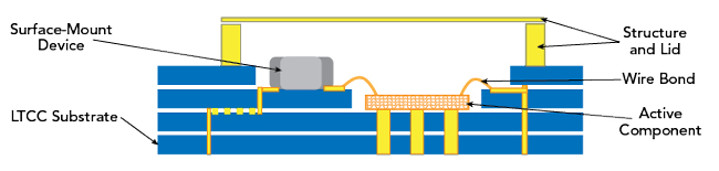
Figure 2 LTCC package cross section.
AiP
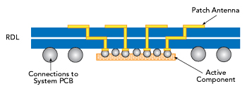
Figure 3 AiP cross section.
AiP technology is a relatively new idea, rapidly gaining popularity, the interest driven by the opportunity of high volume mmWave applications such as 5G smartphones. These systems have a small number of antenna elements which can be integrated into the package with the associated active components (see Figure 3). AiP is not a single package technology, rather a range of approaches, including double-sided assembly, redistribution layers (RDL), integration of passive devices and shielding.4