
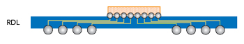
Figure 4 FOWLP cross section.
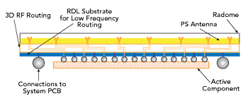
Figure 5 PolyStrata package cross section.
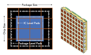
Figure 6 Die to array interconnect.
FOWLP
Similar to AiP, FOWLP is not a single technology. With many different approaches and names, the common idea is enabling a device with high density pads or leads to connect to a printed circuit board (PCB) when the PCB and device cannot directly interconnect. Similar to AiP, this is accomplished using a redistribution layer for routing (see Figure 4).
PolyStrata Packaging
PolyStrata system in package technology is a commercialized technology based on DARPA’s 3D Micro Electromagnetic Radio Frequency Systems program. The technology is a batch additive process that uses copper and air dielectric routing. MMICs and other surface-mount devices can be flip mounted, soldered or wire bonded onto the PolyStrata substrate (see Figure 5). PolyStrata integration offers advantages for mmWave packaging: high isolation routing of the substrate can be used to integrate filters, diplexers and other high performance components, achieving isolation which is challenging at high frequencies. PolyStrata uses a copper substrate which supports microcoax signal routing from DC to >300 GHz, achieving isolation greater than 80 dB. In addition to copper and air, minimal dielectric support structures support the center conductor, and the routing maintains the performance in three dimensions, enabling the design and integration of passive components.
MMWAVE ARRAYS
While these packaging approaches are similar, they have important differences when used for mmWave arrays. First, consider loss. The importance of minimizing loss depends on the application. At lower frequencies and for smaller arrays, loss may not be a significant factor; however, it becomes very important at higher frequencies and in arrays with more elements.
To illustrate, Figure 6 shows a 4 x 4 section of an array with the beamformer IC (BFIC) or MMIC driving the antenna elements. The size of the array elements will depend on frequency; at V-Band, each element is on the order of 2 mm on a side. The figure shows the size difference between the BFIC or MMIC and the antenna array. The mmWave package routes the high frequency signals from the IC to the array, which could be greater than 4 mm in this example. The packaging technology chosen must route both the mmWave, low frequency and DC signals - possibly 16 or so mmWave signals and 5x to 10x more lower frequency signals - from the IC to the antenna array or the system PCB. The packaging designs discussed here use either PCB, RDL, ceramic or PolyStrata for the mmWave routing, and their losses reflect the different transmission line structures used (i.e., stripline, microstrip, coax), substrate thicknesses, etc. Table 1 compares the typical loss of these materials for a 4 mm long transmission line at 60 GHz.
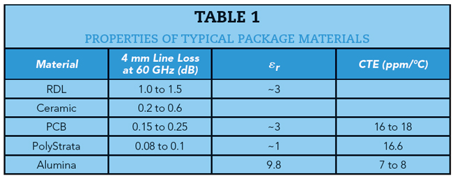
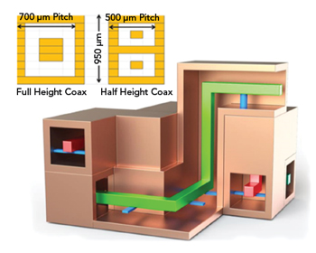
Figure 7 Three-dimensional coaxial structures built with PolyStrata technology.
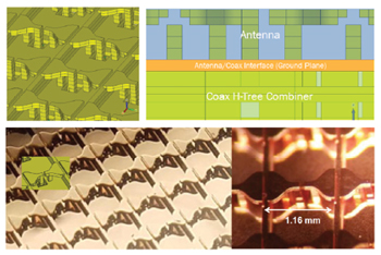
Figure 8 PolyStrata D-Band antenna array and feed network.
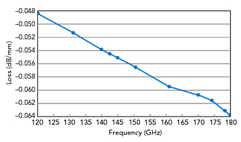
Figure 9 PolyStrata coaxial transmission line loss vs. frequency.
Another important consideration is thermal performance, with two aspects to consider, the first is the thermal resistance from the heat generating component to an interface or external heat sink. For AiP, FOWLP and PolyStrata, the active devices can be coupled through a thermal interface material (TIM) to a heat sink, slug or thermal via. The TIM can be included with a ceramic package and connected to a lid or heatsink, as needed. While this aspect of thermal performance may be similar among the approaches, the second consideration, the coefficient of thermal expansion (CTE) of the package, will differ among the technologies. The CTE must be sufficiently matched between the IC, the package substrate and the PCB to which it is attached; otherwise, the reliability of the attachment will be degraded during thermal cycling. Table 1 includes CTE in the comparison of package substrate materials.
These packaging solutions are designed to route many low frequency and high frequency signals in a small space. It is important to do this while maintaining high electrical isolation among the signals, which will depend on the transmission line structures and the relative dielectric constants (εr) of the respective materials (also shown in Table 1). The mmWave signals are typically routed using microstrip, stripline or substrate integrated waveguide transmission lines, along with vias. An advantage of PolyStrata is the capability to build three-dimensional coaxial structures which are small yet fully shielded (see Figure 7), isolation greater than 80 dB can be achieved at 70 GHz.
All the packaging technologies discussed support heterogeneous integration, i.e., the capability to solder, wire bond or flip chip devices on the substrate. An important consideration is the interconnect pitch. As frequency increases, so does the need for finer pitch interconnects. A bump pitch of 100 μm may be needed at 100 GHz, for example. Further integration is possible with the ceramic and PolyStrata technologies, which enable high performance components such as filters or couplers to be integrated into the substrate. The ability to do this is limited with a PCB substrate.
With any packaging technology, scalability is important. This can be the capability for high volume production with repeatable performance or geometric scalability, i.e., the ability to tile packages to build a larger antenna array. As discussed, these technologies are in production for various applications. Tiling the packages into a larger array depends on the ability to route the signals in the available space while achieving the required loss and isolation. This depends on the system frequency and number of signals, so it is difficult to generalize a comparison.
Another factor for some applications is be the capability to support the antenna element design. PolyStrata has an advantage because of its three-dimensional nature and use of an air dielectric. An example of a PolyStrata antenna array is shown in Figure 8. This 130 to 175 GHz array was fabricated and tested, achieving good performance across the frequency range.5 Other technologies can support two-dimensional structures, for example, a cavity backed aperture coupled patch antenna.6
Finally, as applications move to higher frequencies, the same packaging technology platform chosen for lower frequency systems should remain viable to address all the applications shown in Figure 1. PolyStrata has demonstrated low loss and high isolation through D-Band (see Figure 9), demonstrating better than 0.064 dB/mm loss to 180 GHz. For comparison, a PCB-based approach demonstrated a loss of 0.19 dB/mm at 150 GHz with a microstrip transmission line and 0.18 dB/mm for a grounded coplanar waveguide transmission line.6
SUMMARY
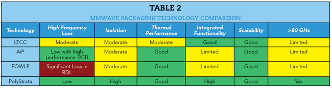
Packaging technologies evolve to support market requirements. As mmWave systems and devices proliferate, the need to package and connect these devices to antennas grows, as well as the complexity of the packaging task. This article has reviewed several popular technologies, each a good solution depending on the system requirements and design approach (see the summary in Table 2). When choosing a packaging platform, consider the operating frequency, number of low and high frequency signals to be routed, the components or functions to be integrated, the type of antenna element and the thermal environment.
References
- Gartner, Small Cells Market Status Report, December 2018.
- I. Nasr et al., “A Highly Integrated 60 GHz 6-Channel Transceiver With Antenna in Package for Smart Sensing and Short-Range Communications,” IEEE Journal of Solid-State Circuits, Vol. 51, No. 9, Sept. 2016, pp. 2066–2076.
- “Imec Adds Machine Learning to 140 GHz Radar Technology,” Microwave Journal, May 22, 2019.
- C. Zwenger and V. Chaudhry, “Antenna in Package (AiP) Technology for 5G Growth,” Chipscale Review, March-April 2020.
- Jared Jordan, et. al., “Monolithically Fabricated 4096-Element, PolyStrata Broadband D-Band Array Demonstrator,” 2019 MTT-S International Microwave Symposium.
- A. Lamminen, J. Säily, J. Ala-Laurinaho, J. de Cos and V. Ermolov, “Patch Antenna and Antenna Array on Multilayer High-Frequency PCB for D-band,” IEEE Open Journal of Antennas and Propagation.