
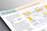
We have released our thin film circuit design guidelines. Designed to help RF, microwave, and millimeter-wave circuit design engineers with optimizing their layouts for our advanced ion beam milling (or etching) process, the layout tolerances and approaches include the following key areas of design for creating optimal Lange couplers, stand-offs, filters, terminations, planar and spiral inductors, and other custom thin film circuits:
- Resistor Length
- Resistor Width
- Conductor Overlap
- Metal Pullback
- Lines and Spaces
- Cut Out Radius
- Laser Cut Features
- Notched Via Edge Wrap
- Edge of Via to Edge of Metallization
- Hole Location
- Hole Spacing
- Hole Dia. Aspect Ration For Plated Vias
- Edge Proximity = Substrate Thickness
- Front to Back Registration
A table details the expected range of values for tantalum-nitride (TaN) and nickel-chromium (NiCr) resistors, titanium-tungsten (Ti or TiW) adhesion layers, nickel (Ni) sputtered palladium or platinum sputtered barrier layers, and gold (Au) conductors.
The design guidelines also include a review of the most common substrate materials used in producing ion beam etched thin film circuits including:
- As fired and polished 99.6% Alumina (Al)
- Polished 99.5% Beryllium Oxide (BeO)
- Polished Aluminum Nitride (Al)
- Polished Fused Silica
- Polished Titanates
Optimized circuit layouts and SemiGen’s sputtering and vacuum deposit process expertise utilizing all these materials, provides the best and most repeatable traces and spaces, and excellent eutectic value and bond strength. Other metal schemes are also available by request or as performance attributes dictate.
Download the guidelines and for additional insight on this subject, download our tech brief “Leveraging the Precision of Ion Beam Milling vs. Chemical Etching Thin Film Circuits”
Additional design-for-manufacturability and support is available by contacting our techincal support team.
![]()