
Thin-film multi-layer multi-chip module with deposited substrate (MCM-D) technology using the system in a package concept is presented as a viable approach for the integration of high performance wireless front-end systems. Due to the high quality dielectrics and copper metallization, high quality inductors are available. This, together with the integrated passives design library containing fully scaleable equivalent models for the inductors, capacitors, resistors, transmission lines and discontinuities, allows easy and accurate design. Examples of bandpass filters, power dividers, quadrature couplers, microwave feedthroughs, a Digitally Enhanced Cordless Telephony (DECT) VCO and a wireless local area network (LAN) LNA are given.
With the current trend in miniaturization of telecommunication devices for portable and battery-powered applications, a high level of integration to reduce size, weight, cost and power consumption is becoming essential. In particular, the radio front-end still contains a large number of discrete components, which are an important bottleneck for further integration. Moreover, the operational frequency of these radio front-ends is rapidly moving into the gigahertz frequencies. To realize high performance front-end systems for wireless applications, a miniaturization and integration technology capable of high frequency and high quality performance is essential. A number of technologies are candidates to fulfill these demanding requirements.
During the last few years, a lot of research has been focused on single-chip (Bi)CMOS RF transceivers. Several trends and developments have led to more integrated transceivers. However, there are still several arguments1 that indicate that a single-chip transceiver in standard digital deep sub-micron CMOS technology is not feasible in the foreseeable future. One of the problems is the unavailability of high-Q on-chip inductors essential for the realization of low loss filters, matching networks and resonators. The Q-factor of inductors in standard (Bi)CMOS is around eight and may be increased to approximately 25 using special non-standard technologies.2 The unavailability of high performance on-chip passives also leads to more difficult designs as it becomes more difficult to achieve the required system specifications.
A second candidate for the integration of wireless front-ends is low temperature co-fired ceramic (LTCC) technology. LTCC is suited for the realization of integrated passive components and for interconnection with active devices. The quality factors of the integrated inductors may go above 60 but only at low RF.3 This is mainly due to the limited quality of the materials, the large tolerances on dimensions of the screen printed conductors and the vertical shrinkage during firing. Miniaturization is achieved by exploiting the three-dimensional capabilities of the technology. However, this three-dimensional configuration causes large modeling difficulties, hereby limiting the use of LTCC for practical circuit design. Photo-lithographic techniques may be used to reduce the accuracy problems,4 but this reduces the claimed cost benefits even more.
A third important candidate for the realization of fully integrated high frequency front-end systems is thin-film multi-layer or MCM-D technology. In this interconnection technology, it is possible to realize integrated passive components with high quality at microwave frequencies.5 As will be presented further, the inductors may have Q-factors of more than 100 at 10 GHz. Moreover, the tolerances and reproducibility are excellent. By combining these passives with surface-mount (wirebond, flip-chip) active devices, fully integrated RF front-end subsystems may be realized.
This article presents the system-on-a-package (SOP) approach, which allows an increase in the integration level of these future wireless transceivers and at the same time reduces the power consumption.
INTEGRATED PASSIVES MCM-D TECHNOLOGY
The described MCM-D technology (the layer built-up is shown in Figure 1) consists of alternating thin layers of photosensitive benzo-cyclobutene (BCB) dielectric (Cyclotene is produced by Dow) and low loss copper metallizations deposited on a borosilicate glass carrier substrate (εr = 6.2, tan δ ≈ 9.104 ). The BCB dielectric has very low dielectric losses (tan δ ≈ 8.104 ), a low dielectric constant (εr = 2.7) and a low moisture absorption. The material is spin coated in 5 µm thin films and then developed and cured. The curing temperature profile of BCB does not exceed 250°C, which is significantly lower than for most other dielectric materials (such as polyimide). The 3 µm-thick copper metal layer is sandwiched between two 30 nm-thick titanium layers rendering good adhesion. This metal layer is realized by electroplating on a thin titanium-copper seed layer. Via-holes through the BCB dielectric allow the connection of the different metal layers. The vias are immediately formed after the developing step and have a typical diameter of 30 µm.

The TaN resistors and Ta2 O5 capacitors are realized immediately on the carrier substrate as they require a high temperature annealing step. This is not compatible with the relatively low temperature steps for the subsequent BCB layers.
SYSTEM-ON-A-PACKAGE APPROACH
The SOP approach is schematically shown in Figure 2. The basic assumption is that it is not possible to integrate complete front-ends on a single-chip as there will always be some subblocks that are difficult to realize (for example, filters and high-Q spirals). The presented approach has the advantage that the most optimal technology (performance/cost) can be used to create each subblock. The passives are integrated as much as possible in the low cost MCM-substrate, hereby reducing the cost of the active chips. Such an approach requires that a complete integrated passives design library is available to allow for an easy co-design between the active and the passive elements.

When different circuits are integrated in close proximity on the MCM, it may be necessary to provide some shielding to prevent radiative coupling between the receiver and transmitter. It may also be required to protect the circuit from the external environment. The shielding is accomplished by putting a metal box on top of the circuit. To connect the inside to the outside world, a specially designed, impedance-controlled, low loss feedthrough is required.
DESIGN LIBRARY AND COMPONENT MODELS
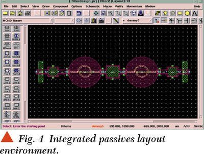
A complete design library with parameterized scaleable models has been created and verified up to 50 GHz.6 The component library is integrated in Agilent's Advanced Design System (ADS) CAE environment, thereby greatly simplifying circuit design. The designer simply clicks on the appropriate component in the library, specifies its values, and drag and drops the component icon in the schematic, as shown in Figure 3. Once the simulated performance is satisfactory, the layout for mask making, shown in Figure 4, is created by clicking the auto-layout button. As models for the passive and active devices are available in the same simulator, a full co-design between the active and passive elements becomes possible.

Transmission Lines and Discontinuities
A coplanar type of transmission line (CPW) is used as this configuration has several advantages over the more traditional microstrip approach: no through-substrate vias are required and backside wafer processing is omitted. The standard coplanar line is located on the middle low loss Cu metal layer.
The 3 µm thick Cu layer is used to build the standard transmission lines. A model has been developed which allows scaling both the width and slot of the CPW transmission lines. The standard 50 Ω lines have a width of 77 µm and a slot of 20 µm, corresponding to a loss of only 0.07 dB/mm at 20 GHz (for comparison a 25/40/25 µm CPW line on GaAs has a loss of 0.18 dB/mm). The standard CPW layer has a useful characteristic impedance range from 40 to 120 Ω. Low impedance lines can be realized by placing the strip on the top metal layer, or by locally shifting to a thin-film microstrip-based approach. Impedance values down to 10 Ω are hereby possible.7 Scaleable models for all common discontinuities (bridges, T-junctions, X-junctions, vias, corners and reflects) are also available.
Capacitors
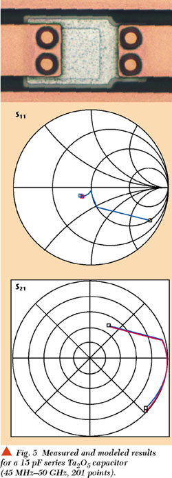
Two types of metal-insulator-metal (MIM) capacitors can be used. For the larger capacitance values (720 pF/mm2 ) a layer of anodised tantalum is realised on the glass carrier substrate. These Ta2 O5 capacitors are contacted with Al-based contact metal. For the small capacitors (5.5 pF/mm2 ) the insulating dielectric is BCB.
The measured versus simulated results for a 15 pF series Ta2 O5 -capacitor are shown in Figure 5. Good correspondence can be observed between measurement and simulation results.
Inductors
High-Q spiral inductors are integrated in the Cu metal layer in a coplanar style. Layouts separately optimized for low cost (corresponding to narrow strips and slots, and a small gap to the ground plane) or high performance (wider strips and slots, and a larger distance to the ground plane) are available.
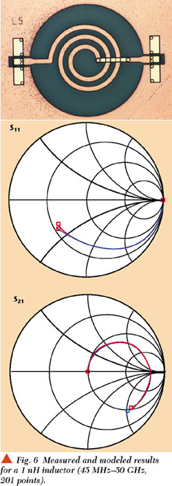
The quality factors of the MCM-D inductors may rise above 100 at 10 GHz (for inductances < 1.7 nH). Of course, for inductors with larger values the quality factor will drop due to the increased losses and capacitive coupling between the turns. For example, an inductor of 18 nH has a Q of 38 at 2 GHz and an inductor of 40 nH has a Q of 29 at 1 GHz. Therefore, the Q values are significantly higher than those that can be achieved on silicon.
The inductors are modeled using higher order models which are able to accurately represent the inductors' S-parameters above the first resonance frequency. The measured and simulated S-parameters are shown in Figure 6. Excellent correspondence can be observed.
Resistors
A transmission line-based model is used to implement resistors since this allows easy and accurate scaling of both the length and width. The obtained accuracy is shown in Figure 7, where the measured and modeled results for a 50 * 100 µm (50Ω) and a 25 * 1000 µm (1000 Ω) series resistor are displayed from 45 MHz to 50 GHz. Excellent correspondence can be observed.

A sheet-resistance of 25 Ω/sq is used, which is very well suited for most microwave applications (such as 50 Ω termination resistors or for stabilizing a transistor stage). For large resistors (for example, DC-biasing resistors), meandered versions are used which allows the required area to be drastically reduced.
PASSIVE CIRCUITS
Bandpass Filter
Figure 8 shows a photograph of a 5.2 GHz bandpass filter implemented in MCM-D. The two 0.625 nH MCM-D inductors have a very high maximum Q of 208 at 14 GHz. At the design frequency of 5.2 GHz, the Q is 127. In the same figure, a comparison between measurements and simulations of the complete filter is shown and excellent agreement can be observed. In addition, the graph shows simulation results indicating the influence of a decreasing inductor Q. With the high-Q inductor, the insertion loss in the passband is 3 dB at 5.16 GHz. When the Q drops to 35 or 24 at 5.2 GHz, the insertion loss of the filter increases to 4.9 dB or 6.2 dB, respectively. This degradation illustrates the importance of high-Q spiral inductors.

Power Dividers
Wilkinson power dividers with different architectures, shown in Figure 9, can also be integrated with very high accuracy and performance. Their characteristics are summarized in Table 1. Figure 10 shows the measured and simulated performance of the distributed design. A near perfect correspondence can be observed up to 50 GHz.


Quadrature Couplers
Ninety degree hybrid couplers are very useful in wireless front-end systems. Distributed realizations have been previously presented.8 A lumped version is shown in Figure 11 that uses two inductors of 1 nH (Q = 83 at 10 GHz). The measured insertion loss is 0.27 dB. The bandwidth of this type of hybrid is very narrow. However, due to the excellent prediction of the models in the design library and good processing accuracy, the target frequency was achieved for all designed couplers in a single processing run.

MICROWAVE FEEDTHROUGHS
As previously indicated, microwave feedthroughs are also an essential requirement for the successful realization of the system in a package approach. Feedthroughs can be realized on the middle and bottom metal layers with very good performance.
Two feedthrough structures are shown in Figure 12, where the CPW line goes underneath a grounded metal plate, representing the grounded metal wall. This assumption has been verified using 3-D simulations.9 A feedthrough realized on the middle metal layer allows for the realization of low loss feedthroughs up to 25 GHz. When the bottom metal layer is used, an excellent return loss can be obtained to above 50 GHz, as shown in Figure 13.


ACTIVE REALIZATIONS
A DECT VCO
A photograph of a VCO module for a DECT application integrated in MCM-D is shown in Figure 14. All 28 passive components are integrated in the interconnection substrate. Four active devices are wirebonded10 to the substrate. In this way, a small system (7.5 mm2 ) is realized, four times smaller than the presently used printed circuit board version. Wirebonding was used because the bare die active devices have contacts at both the top and bottom sides.

The VCO operates at half of the DECT operational frequency because a frequency doubler to 1890 MHz is available in the accompanying RF chip. The measured performance of the VCO indicates 5 dBm output power, 894.5 to 925 MHz (transmit) and 826.5 to 845.3 MHz (receive) tuning range, 10.2 MHz/V (transmit) and 6.1 MHz/V (receive) tuning sensitivity, 117.9 dBc/Hz phase noise at 1.72 MHz from the carrier frequency (limited by the dynamic range of the measurement equipment) and 109.7 dBc/Hz at 100 kHz from the carrier frequency. The phase noise of 117.9 dBc/Hz at 1.72 MHz from the carrier frequency is 14.9 dB better than the DECT specifications. This achievement may be attributed to the excellent high-Q integrated spiral inductors and capacitors.
5.2 GHz Wireless LAN Low Noise Amplifier
A photograph of a low noise amplifier (LNA) for 5.2 GHz wireless LAN is shown in Figure 15. All passive components for matching and biasing are integrated in the MCM-D substrate. Bandpass filters before and after the amplifier stage (for use in a superheterodyne architecture) are also included. This makes 23 integrated passives in total.

The active device is a commercial GaAs pHEMT, flip-chip mounted on the MCM using gold stud bumps. The LNA was optimized for high gain performance. The LNA characteristics without bandpass filters include a noise figure below 2.4 dB, gain of 12.9 dB, 1 dB compression point of 5 dBm at the input and power consumption of 28 mW (14 mA with 2 V). Measurements with the bandpass filters are also shown. The noise figure with the filters becomes 5.4 dB, with a gain of 6.8 dB, input matching < 9 dB and output matching < 15 dB. This performance is better than what may be achieved with similar integrated solutions in silicon (including integrated bandpass filters).
CONCLUSION
Thin-film MCM-D proves to be an excellent technology for the integration of high-Q spiral inductors and passive components in general. The technology, SOP approach, design library and component models have been discussed. Examples have been given of narrowband bandpass filters, Wilkinson power dividers, quadrature couplers, a DECT VCO and a wireless LAN LNA. Very good performance has been obtained each time due to the high quality of the components. The measurements are also in very good agreement with the simulations, indicating the high accuracy of the design library.
ACKNOWLEDGMENT
This work was partially supported by grants from the Office of Naval Research and the National Science Foundation. The material for this article was first presented at the RAWCON2000 IEEE Radio and Wireless Conference held in Denver, CO in September 2000. *
References
1. S. Donnay, P. Pieters, K. Vaesen, W. Diels, P. Wambacq, W. De Raedt, E. Beyne, M. Engels and I. Bolsens, "Chip-package Co-design of a 5 GHz RF Front-end," IEEE Proceedings, 2000.
2. J.N. Burghartz, "Spiral Inductors and Transmission Lines in Silicon Technology Using Copper-damaschene Interconnects and Low Loss Substrates," IEEE Transactions on Microwave Theory and Techniques, Vol. 45, 1997, pp. 19611968.
3. J. Muller, "High-quality RF-inductors in LTCC," Proceedings of ISHM International Symposium on Microelectronics, Minneapolis, 1996.
4. P. Barnwell, "Microwave MCM-C Utilizing Low Loss LTCC and Photo-patterning Processes," Microwave Journal, Vol. 42, 1999.
5. G. Carchon, S. Brebels, K. Vaesen, P. Pieters, D. Schreurs, S. Vandenberghe, W. De Raedt, B. Nauwelaers and E. Beyne, "Accurate Measurement and Characterization of MCM-D Integrated Passives up to 50 GHz," International Conference and Exhibition on High Density Interconnect and Systems Packaging, Denver, CO, 2000, pp. 307312.
6. G. Carchon, P. Pieters, K. Vaesen, S. Brebels, D. Schreurs, S. Vandenberghe, W. De Raedt, B. Nauwelaers and E. Beyne, "Design-oriented Measurement-based Scaleable Models for Multilayer MCM-D Integrated Passives. Implementation in a Design Library Offering Automated Layout," International Conference and Exhibition on High Density Interconnect and Systems Packaging, Denver, CO, 2000,
pp. 196201.
7. G. Carchon, S. Brebels, W. De Raedt and B. Nauwelaers, "Design of Distributed Elements in Ku-band in Coplanar-waveguide Based MCM-D," Electronic Components and Technology Conference, Las Vegas, NV, 2000, pp. 15541559.
8. G. Carchon, W. De Raedt and B. Nauwelaers, "Integrated Wilkinson Power Dividers in C-, Ku- and Ka-band in Multi-layer Thin-film MCM-D," European Microwave Conference, Paris, France, 2000, pp. 171174.
9. G. Carchon, O. Di Monaco, K. Vaesen, S. Brebels, W. De Raedt and B. Nauwelaers, "Design and Characterization of CPW Feedthroughs in Multi-layer Thin-film MCM-D," RAWCON, Denver, CO, 2000, pp. 167170.
10. K. Vaesen, P. Pieters, G. Carchon, W. De Raedt, E. Beyne, A. Naem and R. Kohlmann, "Integrated Passives for a DECT VCO," International Journal of Microcircuits and Electronic Packaging, Vol. 23, 2000.