
Multichannel antenna arrays are key enablers in the next generation of defense and wireless communications systems, for beam steering and multiple-input-multiple-output (MIMO) architectures. They allow both electronic warfare (EW) and consumer systems to provide precise, dynamically allocated and robust service levels, supporting mobility business models that were unthinkable a few years ago. Approaching this new technological complexity begins in R&D, where similar breakthroughs in design tools and verification methodologies can address phased array beam forming challenges efficiently, in a lean commercial environment. This article shows how a connected suite of standard tools can streamline the design process while enabling trade-offs in RF and digital beam forming performance.
Multi-antenna techniques such as beam forming (RF, digital and hybrid) and massive MIMO are now major trends in 5G and satellite communications systems and EW, thanks to their ability to provide precise, dynamically allocated and robust service levels. These techniques solve different problems at the system level and can be used together to deliver more bits per Hz in a crowded area, with less interference. What has enabled these elaborate technologies to advance from their use in specialized military applications to low cost, high volume consumer-oriented platforms, over the course of just a few years? The answer lies with semiconductor improvements gained in keeping with Moore’s Law, specifically reduced cost, size and power and increased bandwidth and microwave performance. Consumer demand is playing a role in driving beam forming and MIMO into the commercial sector, leading to mobility business models that were unthinkable only a few years ago.
For all the good that comes with these technologies, their complexity creates challenges, especially with the design of phased arrays. Overcoming these challenges to achieve an optimal system design requires a new, top-down system-level methodology, one that streamlines the design process, from assessing beam forming strategies and system-level scenarios to system implementation.
PHASED ARRAY DESIGN CHALLENGES
When designing phased array systems, several design flow challenges — both technical and economic — must be addressed. For example, to gain a system perspective of the economic and service-level trade-offs, the impact of realistic analog, electromagnetic (EM) and digital signal processing (DSP) performance must be considered. However, a system perspective is often hard to achieve. One challenge is the sheer number of engineering disciplines required to develop a phased array, most operating independently. Different toolsets are used for analyzing antennas and EM, RF transceivers and manifolds (which can take the form of ICs, modules and boards), as well as the integration of RF, digital and hybrid beam forming architectures — which cross boundaries between the baseband ASIC/FPGA and RF architectures.
While beamwidth and sidelobe levels are typical measures of array performance, the larger goal of any phased array subsystem is delivering higher system-level performance. Beam forming is used to concentrate RF power in specific directions, which reduces the RF power needed to achieve a given link quality (e.g., data throughput). Secondly, this also reduces interference for other users while improving their link quality and conserving battery life. At a higher level, the underlying RF impairments of the array affect the final sidelobe levels and beam patterns, reducing system-level performance.
In phased array transmitters, sidelobe levels from imperfectly formed beams may interfere with external devices or make the transmitter visible to countermeasures. In radar systems, sidelobes may also cause a form of self-induced multipath, where multiple copies of the same radar signal arrive from different sidelobe directions. These additional propagation paths can exaggerate ground clutter and must be removed with sophisticated DSP algorithms. Degraded RF array performance can also misdirect the main beam, widen it or reduce its directivity. Examples of this are “squinting,” (e.g., frequency dependent beam distortion that occurs during each radar chirp, as shown in Figure 1) and AM-AM/AM-PM distortion. In a military system, the reduction in effective radiated power (ERP) reduces the power illuminating a distant target and its probability of detection and effective standoff range. For communication link budgets, the effect is on the signal-to-noise ratio (SNR) and coverage area.
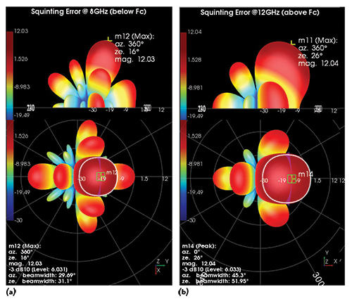
Figure 1 Array antenna patterns at 8 GHz (a) and 12 GHz (b) showing beam squinting and sidelobe variation.
In phased array receivers, poor RF array performance may add noise. It may also increase reception from unwanted directions, from sidelobes and misplaced nulls, or widened beams from overloading. These effects reduce sensitivity and range, increase susceptibility to interferers or jammers and degrade the overall error vector magnitude (EVM), bit error rate (BER) and throughput (or probability of detection). Gain/Temperature (G/T) is a common measurement for receiver arrays, combining several underlying degradations into a composite figure-of-merit (similar to SNR) over a range of received spherical angles (see Figure 2). The array may be programmed to “listen” in a certain direction, yet how well does it achieve that goal?

Figure 2 G/T analysis for a T/R module, showing sidelobes and directivity.
Although MIMO techniques are related to beam forming, they have subtly different issues from forms of crosstalk and correlation. Depending on the architecture, these techniques may be used in tandem on the same platform. MIMO improves the robustness of communication links in dense mobility environments, while improving spectral efficiency. Since MIMO requires individually-addressable signal paths for each “stream,” the cost and power of the digital-to-analog and analog–to-digital converters (DAC and ADC) and dedicated signal processing adds dramatically to the size, weight and power (SWaP) of the array subsystem. Functionally, analyzing multiple data streams from a single user (MIMO), compared to individual data streams from multiple users in a multi-function array, requires the array and its impairments to be accessed at the higher system-level.
In hybrid beam forming (HBF) and composite arrays comprised of multiple single-function sub-arrays, the likelihood of self-interference increases. HBF is gaining popularity in the 5G community as it allows cost-benefit trades between analog beam forming (ABF) and digital beam forming (DBF). In HBF, there are still multiple distinct baseband signals, but they drive ganged sub-arrays at the RF beam forming levels; these sub-arrays perform phase shifting at the transmit carrier frequency. Splitting the functionality achieves both directionality (beam forming) and throughput (MIMO) at lower cost and power from RF ASICs, ADCs and DACs.
A final concern is whether physically imperfect arrays really work across their intended bandwidths at their microwave or millimeter wave carrier frequencies and in their propagation environments. Until recently, this has been difficult for a disjointed set of simulation tools to predict, requiring dependence on hardware prototyping. Each engineering group has its own established tool chains and methodologies which are difficult to combine across disciplines. Back annotating engineering changes up to the system level is also difficult.
Collectively, the number of toolsets for architecting and validating phased arrays is daunting and needs much investigation and improvement. Given these challenges, a predictive, system-level design flow can greatly reduce iterations and the need for hardware validation, indoor/outdoor antenna ranges and flight time.
In addition to these design flow challenges, there are softer design flow risks to consider: In some environments, intellectual property (IP) is concentrated in people rather than tools. Preserving and re-using design experience and project IP is a strategic concern. Issues like controlling R&D “overhead” costs not assigned to a contract, technology turnover, time-to-deployment and high skill requirements add to the demand for streamlined model-based engineering (MBE) across multiple domains.
ADDRESSING THE CHALLENGES
Established electronic design automation (EDA) tool chains from companies like Keysight are being expanded to improve coverage for systems that use phased arrays and beam forming. These expanded tool chains help address several issues that arise from the use of disjointed design flows:
Choosing the right level of abstraction. Finding the right level of simulation abstraction, especially in the RF design flow, can be difficult. If the models are too idealized for speed, then the simulations will not be accurate. That leads to increased hardware validation and cost. On the other hand, if excessive physical detail is included, the huge simulations will be too slow to validate meaningful portions of a “test plan” and not very scalable beyond 100-element arrays. Fortunately, there is a middle ground. Behavioral modeling balances the many orders of simulation magnitude between multi-user 5G and radar system scenarios, with active signaling, beam forming algorithms, nonlinear RF T/R modules and EM solver physical design details. Intelligent choices about “which powers of 10” to combine can make the flow scalable to thousands of array elements and unite the teams, while still preserving essential accuracy.
Scaling up to size. Once the right level of abstraction is found, the next step is applying it to larger arrays (>1000 elements). Although spreadsheets are often used for architecture studies, they give up too much flexibility and do not consider noise, nonlinearities, X-parameters®, component variations and statistics, frequency dependence, mismatch or other factors. Circuit-level tools can be “brute forced” into array analysis, but that comes at a huge price for usability and speed. Instead, an intermediate modeling level can be used where nonlinear, multi-stage arrays are modeled in seconds using a simple use model, preserving the idea of “predictive” accuracy (i.e., a simulation that will tell you something you didn’t already know).
Validating the rendered beam (baseband with realistic RF). The ability to drive the accurate RF array model, from the previous steps, with realistic baseband beam forming algorithms is necessary to validate the beam integrity of the array under a range of 3D array configurations, scan angles, windowing tapers, sub-array partitioning, operating frequencies and other conditions. MATLAB algorithms by themselves do not save design iterations without some level of RF accuracy informed from the actual design process. Conversely, without complex algorithmic behaviors and baseband corrections, the benefit of static RF models can only be inferred at the array subsystem. Both domains must work together to predict the performance of the whole subsystem and reduce the cost of prototyping and test.
Handling dynamic, system-level scenarios. Array subsystems are designed to deliver a certain level of system performance, whether a 5G, EW or emerging satellite platform. A given array subsystem must be validated with format-realistic signaling and receiver processing in dynamic scenarios to ensure it is compliant with published standards, interoperable with other equipment under specified conditions and meets other performance minimums. Most organizations wait until operational hardware prototypes are available to do this validation, which typically requires access to indoor and outdoor test ranges, flight time and other expensive assets. This leads to late discovery and troubleshooting of architectural flaws at the pilot production stage. A connected, top-down, system-level design flow enables diagnosing and quickly addressing “preventable” errors before requiring more rigorous testing; expensive assets are only needed at the end. The connection of “proposal” to “final design,” in the terms of the customer’s own delivered performance, makes this step worth pulling into the R&D phase, as part of a soft, simulation-based test plan.
This final point has a large economic payoff. However, the following three capabilities are required to realize the benefits of a unified phased-array workflow:
- Exchanging design information — From an MBE perspective, a team works from the top down within a single discipline, such as moving beam forming algorithms from floating point into working FPGAs or ASICs. From the system perspective, maintaining this MBE approach across disciplines requires additional tool connectivity that is less common. Humans become the design flow bridge, often using word processors and spreadsheets in lieu of design files; however, this requires interpretation that inserts risk into the process. Direct exchange of design information enables faster cross-validation and engineering changes to back-propagate to the system architect, in the event of a lower level technical (or material) change. Design information formats include MATLAB models, System C/C++, VHDL and Verilog, S- and X-parameters, SysParameters, 3DEM far field pattern files and waveform files.
- External scripting and automation for formalized cross-validation — An environment like Keysight’s SystemVue can be used to assemble meaningful baseband-RF co-validation scenarios. These scenarios are automated with external applications to run a regular regression harness of automated verifications, such as for a nightly build process. The ability to cross-validate a project continuously, from the very first day, improves transparency, enables better project management and lowers risk.
- Integration with test — Finally, design simulation is helpful, yet it often remains separate from real world integration, variations and results. The ability to connect the EDA world directly to wideband, multi-channel test and measurement, with support for real-time prototyping and instrument personalities, means that design insight can be preserved in a closed modeling loop using a consistent approach, from proposal into hardware. Combining simulation with versatile software-defined measurement platforms allows earlier architecture validation and enables flexible verification strategies that reduce project cost and increase utilization of test assets.
Progress in each of these areas is possible using a design flow that connects tools and reference IP in several domains into an open flow. Keysight SystemVue, for example, provides a phased-array design personality and can also operate as a co-validation backplane. The following case studies show how a unified, model-based design approach for phased arrays might work in the real world.
EW ARRAY
Consider a basic EW scenario in which a central monostatic radar beam forms in “tracking” mode to follow a radar cross section (RCS) target, such as an aircraft, as it flies in a path around a city, using latitude, longitude, altitude waypoints. As the position of the RCS target moves, both the transmitter and receiver arrays are steered to follow its direction. The arrays are each 25 × 25 uniform rectangular with a Taylor taper, whose complex weights are dynamically updated at the system level using adaptive algorithms. The arrays can either be purely behavioral or incorporate some effects from a T/R module chain modeled in an RF simulation domain. In Figure 3, the range-Doppler bins are shown at the system level, along with the beam quality.
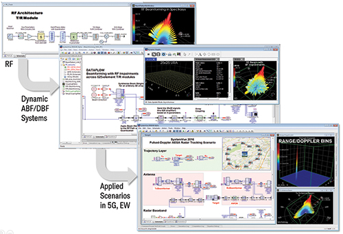
Figure 3 System analysis using multiple platforms, from the RF components to end use scenarios.
In the RF array, it is possible to account for the X-parameters of components, designed in ADS or measured on the bench. It is also possible to account for noise, nonlinearities, mismatch and frequency response, as well as the use of quantized phase, delay or amplitude states. Coupling between array elements, based on a true EM simulation, and realistic far field patterns for the radiating elements may be taken into account in the final, working beam patterns. As the array scans to more extreme angles, the scan loss and grating lobes degrade the performance. If the highest accuracy is needed for troubleshooting, a few key RF pieces may be directly co-simulated with the ADS circuit envelope/Ptolemy simulators — although for larger arrays, a comprehensive co-simulation approach can be impractical. For baseband, if FPGA algorithms are being co-verified, key algorithms can be co-simulated with either an HDL simulator, a Xilinx Virtex 7 FPGA board running in hardware-in-the-loop (HIL) mode or even an instrument. To account for atmospheric fading and terrain, SystemVue can be scripted to connect with the STK software from Analytical Graphics Inc. (AGI). This allows key time-varying quantities like range delay, Doppler shift and propagation loss to be rendered with accurate, fully-coded radar signaling.
With this verification backplane, it is possible to design the phased array and use it in a meaningful, scripted scenario that validates a range of conditions, statistical variations or countermeasures. In this way, an entire organization can contribute files and IP to a common tool and cross validate all the way to the test bench.
5G ARRAY
A likely 5G scenario comprises a wideband, 28 GHz MIMO OFDM link between a planar 4 × 4 array at the base station (i.e., eNodeB) and a 4 × 1 array at the user’s equipment (UE). The beams are dynamically steered using hybrid beam forming (see Figure 4). The link is faded through a millimeter wave 3D MIMO fading model, based on 5G research at New York University. The baseband reference designs for the transmitter and receiver provide the OFDM framing and resource mapping on a flexible level; these designs go beyond LTE-A and include receiver synchronization and demodulation back to the data payload. This complex BER/throughput example includes the effect of the array, beam forming accuracy and an industry-standard fading model. As more UEs and interferers are added, the adaptive beam forming algorithms, the modulation and coding strategy, as well as the RF architecture can be assessed. In this scenario, the flexibility to conduct system-level research, while using a practical RF basis to perform the modeling, allows the system architect to assess how large of an array is needed, the required performance and the risk to the company.
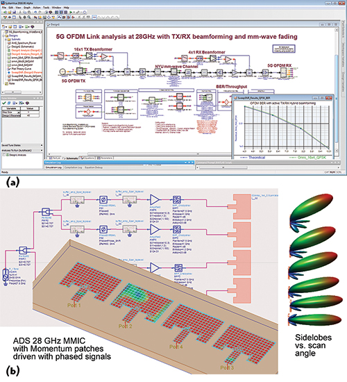
Figure 4 Link analysis of 28 GHz 5G OFDM link (a) and 4 × 1 receive array modeled in Momentum (b).
Conclusion
The practical design challenges for phased array subsystem design go beyond simple technical performance issues associated with individual RF component design. A view of the subsystem’s performance can directly assess overall performance margins across baseband and RF and help designers make trade-offs between the domains, while delivering realistic performance. The critical capability is tying together the circuit simulators, beam forming and DSP algorithms, antenna patterns, system scenarios, FPGA implementations and test equipment in a unified model-based design flow. This can be accomplished using an electronic system-level platform like SystemVue. The resulting connected suite of standard tools helps to significantly streamline the design process. Adding a phased array beam forming personality adds more power, unlocking cross-functional insight.
5G App Note:
For more information, visit http://literature.cdn.keysight.com/litweb/pdf/5992-1448EN.pdf